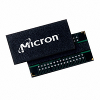
MT47H64M8CB-5E:B Micron Technology Inc, MT47H64M8CB-5E:B Datasheet - Page 127

MT47H64M8CB-5E:B
Manufacturer Part Number
MT47H64M8CB-5E:B
Description
IC DDR2 SDRAM 512MBIT 5NS 60FBGA
Manufacturer
Micron Technology Inc
Datasheet
1.MT47H64M8CB-5EB.pdf
(133 pages)
Specifications of MT47H64M8CB-5E:B
Format - Memory
RAM
Memory Type
DDR2 SDRAM
Memory Size
512M (64M x 8)
Speed
5ns
Interface
Parallel
Voltage - Supply
1.7 V ~ 1.9 V
Operating Temperature
0°C ~ 85°C
Package / Case
60-FBGA
Lead Free Status / RoHS Status
Lead free / RoHS Compliant
Available stocks
Company
Part Number
Manufacturer
Quantity
Price
Company:
Part Number:
MT47H64M8CB-5E:B
Manufacturer:
MICRON
Quantity:
12 388
Company:
Part Number:
MT47H64M8CB-5E:B
Manufacturer:
Micron Technology Inc
Quantity:
10 000
Company:
Part Number:
MT47H64M8CB-5E:B TR
Manufacturer:
Micron Technology Inc
Quantity:
10 000
PDF: 09005aef8117c18e, Source: 09005aef8211b2e6
512MbDDR2_2.fm - Rev. K 8/06 EN
11. The intent of the “Don’t Care” state after completion of the postamble is that the DQS-
12. This is not a device limit. The device will operate with a negative value, but system
13. It is recommended that DQS be valid (HIGH or LOW) on or before the WRITE com-
14. The refresh period is 64ms (commercial) or 32ms (industrial). This equates to an aver-
15. Referenced to each output group: x4 = DQS with DQ0–DQ3; x8 = DQS with DQ0–DQ7;
16. CK and CK# input slew rate is referenced at 1 V/ns (2 V/ns if measured differentially).
17. The data valid window is derived by achieving other specifications:
18. READs and WRITEs with auto precharge are allowed to be issued before
19. V
20.
21. The minimum internal READ to PRECHARGE time. This is the time from the last 4-bit
22. Operating frequency is only allowed to change during self refresh mode (see Figure 54
23. ODT turn-on time
24. ODT turn-off time
25. This parameter has a two clock minimum requirement at any
driven signal should either be HIGH, LOW, or High-Z, and that any signal transition
within the input switching region must follow valid input requirements. That is, if
DQS transitions HIGH (above V
V
performance could be degraded due to bus turnaround.
mand. The case shown (DQS going from High-Z to logic LOW) applies when no
WRITEs were previously in progress on the bus. If a previous WRITE was in progress,
DQS could be HIGH during this time, depending on
age refresh rate of 7.8125µs (commercial) or 3.9607µs (industrial). However, a
REFRESH command must be asserted at least once every 70.3µs or
ensure all rows of all banks are properly refreshed, 8,192 REFRESH commands must
be issued every 64ms (commercial) or 32ms (industrial).
x16 = LDQS with DQ0–DQ7; and UDQS with DQ8–DQ15.
t
tion to the clock duty cycle and a practical data valid window can be derived.
satisfied since
on page 105.
t
rounded up to the next integer.
to the
with
(4) clocks = 8 clocks.
prefetch begins to when the PRECHARGE command can be issued. A 4-bit prefetch is
when the READ command internally latches the READ so that data will output CL
later. This parameter is only applicable when
faster than 533 MHz when
2 applies.
ically delay the internal PRECHARGE command until
on page 71), precharge power-down mode, or system reset condition (See “Reset
Function” on page 72). SSC allows for small deviations in operating frequency, pro-
vided the SSC guidelines are satisfied.
begins to turn on. ODT turn-on time
on. Both are measured from
ODT turn off time
t
DQSQ, and
DAL = (nWR) + (
AOFD.
IH
IL
/V
[
DC
t
IH
WR programmed to four clocks would have
t
]) prior to
WR parameter stored in the MR[11, 10, 9]. For example, -37E at
DDR2 overshoot/undershoot. See “AC Overshoot/Undershoot Specification”
t
RAS (MIN) also has to be satisfied as well. The DDR2 SDRAM will automat-
t
QH (
t
RAS lockout feature is supported in DDR2 SDRAM.
t
t
RP/
DQSH (MIN).
t
QH =
t
t
t
AOF (MAX) is when the bus is in High-Z. Both are measured from
AON (MIN) is when the device leaves High-Z and ODT resistance
AOF (MIN) is when the device starts to turn off ODT resistance.
t
CK). Each of these terms, if not already an integer, should be
t
HP -
127
t
RTP = 7.5ns. If
t
AOND.
t
QHS). The data valid window derates in direct propor-
IH
t
CK refers to the application clock period; nWR refers
[
DC
Micron Technology, Inc., reserves the right to change products or specifications without notice.
] MIN), then it must not transition LOW (below
t
AON (MAX) is when the ODT resistance is fully
t
512Mb: x4, x8, x16 DDR2 SDRAM
RTP / (2 x
t
RTP / (2 x
t
DAL = 4 + (15ns/3.75ns) clocks = 4 +
t
t
DQSS.
CK) ≤ 1, then equation AL + BL/
t
RAS (MIN) has been satisfied.
t
CK) > 1, such as frequencies
©2004 Micron Technology, Inc. All rights reserved.
t
CK.
t
t
RFC (MAX). To
HP (
t
CK = 3.75ns
t
RAS (MIN) is
t
CK/2),
Notes


