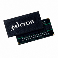
MT47H64M8CB-5E:B Micron Technology Inc, MT47H64M8CB-5E:B Datasheet - Page 86

MT47H64M8CB-5E:B
Manufacturer Part Number
MT47H64M8CB-5E:B
Description
IC DDR2 SDRAM 512MBIT 5NS 60FBGA
Manufacturer
Micron Technology Inc
Datasheet
1.MT47H64M8CB-5EB.pdf
(133 pages)
Specifications of MT47H64M8CB-5E:B
Format - Memory
RAM
Memory Type
DDR2 SDRAM
Memory Size
512M (64M x 8)
Speed
5ns
Interface
Parallel
Voltage - Supply
1.7 V ~ 1.9 V
Operating Temperature
0°C ~ 85°C
Package / Case
60-FBGA
Lead Free Status / RoHS Status
Lead free / RoHS Compliant
Available stocks
Company
Part Number
Manufacturer
Quantity
Price
Company:
Part Number:
MT47H64M8CB-5E:B
Manufacturer:
MICRON
Quantity:
12 388
Company:
Part Number:
MT47H64M8CB-5E:B
Manufacturer:
Micron Technology Inc
Quantity:
10 000
Company:
Part Number:
MT47H64M8CB-5E:B TR
Manufacturer:
Micron Technology Inc
Quantity:
10 000
Table 24:
Figure 66:
PDF: 09005aef8117c18e, Source: 09005aef8211b2e6
512MbDDR2_2.fm - Rev. K 8/06 EN
Parameter
DC input signal voltage
DC differential input voltage
AC differential input voltage
AC differential cross-point voltage
Input midpoint voltage
Differential Input Logic Levels
All voltages referenced to V
Differential Input Signal Levels
Notes:
Notes:
1. V
2. V
3. V
4. The typical value of V
5. V
@ V
1. This provides a minimum of 850mV to a maximum of 950mV and is expected to be V
2. TR and CP must cross in this region.
3. TR and CP must meet at least V
4. TR and CP must have a minimum 500mV peak-to-peak swing.
5. TR and CP may not be more positive than V
6. For AC operation, all DC clock requirements must also be satisfied.
7. Numbers in diagram reflect nominal values (V
8. TR represents the CK, DQS, RDQS, LDQS, and UDQS signals; CP represents CK#, DQS#,
DD
CK#, DQS, DQS#, LDQS, LDQS#, UDQS, UDQS#, and RDQS, RDQS#.
is the true input (such as CK, DQS, LDQS, UDQS) level and V
(such as CK#, DQS#, LDQS#, UDQS#). The minimum value is equal to V
ential input signal levels are shown in Figure 66.
is the true input (such as CK, DQS, LDQS, UDQS, RDQS) level and V
input (such as CK#, DQS#, LDQS#, UDQS#, RDQS#). The minimum value is equal to V
V
and V
differential input signals must cross, as shown in Figure 66.
the true input (CK, DQS) level and V
expected to be approximately 0.5 x V
RDQS#, LDQS#, and UDQS# signals.
Q = 1.8V
IN
ID
ID
IL
MP
- 0.30V
1.075V
0.725 V
0.9V
(
(
(
(
2.1V
AC
DC
DC
AC
(
CP
TR
DC
), as shown in Table 23 on page 85.
8
IX
8
) specifies the allowable DC execution of each input of differential pair such as CK,
) specifies the input differential voltage | V
) specifies the input differential voltage | V
) specifies the input differential common mode voltage (V
(
AC
SS
) is expected to track variations in V
Symbol
V
Input Electrical Characteristics and Operating Conditions
V
V
V
V
MP
IN
ID
ID
IX
X
(
(
(
(
(
DC
DC
AC
AC
DC
)
)
)
)
)
IX
0.50 x V
(
AC
) is expected to be about 0.5 x V
86
–300
Min
250
500
850
DD
ID
(
Q - 175
DC
) MIN when static and is centered around V
CP
DD
is the complementary input (CK#, DQS#). V
Micron Technology, Inc., reserves the right to change products or specifications without notice.
Q.
DD
0.50 x V
X
512Mb: x4, x8, x16 DDR2 SDRAM
Q + 0.3V or more negative than V
DD
DD
V
V
V
Q = 1.8V).
TR
TR
DD
DD
DD
Q. V
Max
Q + 300
Q + 600
Q + 600
- V
- V
950
DD
IX
CP
CP
Q + 175
(
AC
| required for switching, where V
| required for switching, where V
) indicates the voltage at which
DD
CP
Q of the transmitting device
is the complementary input
©2004 Micron Technology, Inc. All rights reserved.
TR
CP
V
V
V
+ V
MP(DC)
IN(DC)
IN(DC)
is the complementary
Units
IH
mV
mV
mV
mV
mV
CP
(
1
DC
MAX 5
MIN
)/2 where V
V
) - V
IX(AC)
5
2
IL
MP
SS
(
V
DC
ID(DC)
MP
(DC).
- 0.3V.
Notes
). Differ-
IH
(
V
3
TR
DD
DC
ID(AC)
1
2
3
4
5
(
AC
is
) is
Q/2.
4
) -
TR
TR


