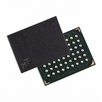
MT48H4M16LFB4-10 TR Micron Technology Inc, MT48H4M16LFB4-10 TR Datasheet - Page 17

MT48H4M16LFB4-10 TR
Manufacturer Part Number
MT48H4M16LFB4-10 TR
Description
IC SDRAM 64MBIT 100MHZ 54VFBGA
Manufacturer
Micron Technology Inc
Datasheet
1.MT48H4M16LFB4-10.pdf
(54 pages)
Specifications of MT48H4M16LFB4-10 TR
Format - Memory
RAM
Memory Type
Mobile SDRAM
Memory Size
64M (4M x 16)
Speed
100MHz
Interface
Parallel
Voltage - Supply
1.7 V ~ 1.9 V
Operating Temperature
0°C ~ 70°C
Package / Case
54-VFBGA
Lead Free Status / RoHS Status
Lead free / RoHS Compliant
NOTE:
NOTE:
pdf: 09005aef80a63953, source: 09005aef808a7edc
Y25L_64Mb_2.fm - Rev. E 11/04 EN
COMMAND
COMMAND
ADDRESS
ADDRESS
Figure 10: Consecutive READ Bursts
COMMAND
COMMAND
Figure 11: Random READ Accesses
ADDRESS
ADDRESS
CLK
CLK
DQ
DQ
CLK
CLK
DQ
DQ
T0
T0
BANK,
BANK,
COL n
COL n
READ
READ
Each READ command may be to any bank.
DQM is LOW.
Each READ command may be to any bank.
DQM is LOW.
CAS Latency = 2
T0
T0
BANK,
COL n
BANK,
COL n
READ
READ
CAS Latency = 2
CAS Latency = 3
T1
T1
NOP
NOP
CAS Latency = 3
T1
T1
BANK,
BANK,
READ
COL a
READ
COL a
T2
T2
NOP
NOP
D
OUT
n
T2
T2
BANK,
READ
COL x
READ
BANK,
COL x
D
OUT
n
T3
T3
NOP
NOP
n + 1
D
D
OUT
T3
TRANSITIONING DATA
OUT
n
T3
BANK,
COL m
READ
READ
BANK,
COL m
D
D
OUT
OUT
a
n
TRANSITIONING DATA
T4
T4
READ
BANK,
READ
BANK,
COL b
COL b
X = 1 cycle
n + 2
n + 1
D
D
OUT
OUT
T4
T4
NOP
NOP
X = 2 cycles
D
D
OUT
x
OUT
a
T5
T5
NOP
NOP
n + 2
n + 3
D
D
OUT
T5
T5
OUT
NOP
NOP
D
D
m
OUT
OUT
x
T6
T6
NOP
NOP
DON’T CARE
n + 3
D
D
OUT
OUT
T6
b
NOP
DON’T CARE
D
OUT
m
T7
NOP
D
OUT
b
17
shown in Figure 12, READ to WRITE, and Figure 13,
READ to WRITE with Extra Clock Cycle, on page 18.
The DQM signal must be asserted (HIGH) at least two
clocks prior to the WRITE command (DQM latency is
two clocks for output buffers) to suppress data-out
from the READ. Once the WRITE command is regis-
tered, the DQ will go High-Z (or remain High-Z),
regardless of the state of the DQM signal, provided the
DQM was active on the clock just prior to the WRITE
command that truncated the READ command. If not,
the second WRITE will be an invalid WRITE. For exam-
ple, if DQM was LOW during T4 in Figure 14, READ to
PRECHARGE, on page 18, then the WRITEs at T5 and
T7 would be valid, while the WRITE at T6 would be
invalid.
WRITE command (DQM latency is zero clocks for
input buffers) to ensure that the written data is not
masked. Figure 13, READ to WRITE with Extra Clock
Cycle, shows the case where the clock frequency allows
for bus contention to be avoided without adding a
NOP cycle, and Figure 13 shows the case where the
additional NOP is needed. A fixed-length READ burst
may be followed by, or truncated with, a PRECHARGE
command to the same bank (provided that auto pre-
charge was not activated), and a full-page burst may
be truncated with a PRECHARGE command to the
same bank. The PRECHARGE command should be
issued x cycles before the clock edge at which the last
desired data element is valid, where x equals the CAS
latency minus one. This is shown in Figure 14 for each
possible CAS latency; data element n + 3 is either the
last of a burst of four or the last desired of a longer
burst. Following the PRECHARGE command, a subse-
quent command to the same bank cannot be issued
until
time is hidden during the access of the last data ele-
ment(s).
completion, a PRECHARGE command issued at the
optimum time (as described above) provides the same
operation that would result from the same fixed-length
burst with auto precharge. The disadvantage of the
PRECHARGE command is that it requires that the
command and address buses be available at the
appropriate time to issue the command; the advantage
of the PRECHARGE command is that it can be used to
truncate fixed-length or full-page bursts.
The DQM input is used to avoid I/O contention, as
The DQM signal must be de-asserted prior to the
In the case of a fixed-length burst being executed to
t
Micron Technology, Inc., reserves the right to change products or specifications without notice.
RP is met. Note that part of the row precharge
MOBILE SDRAM
©2003 Micron Technology, Inc. All rights reserved.
64Mb: x16


