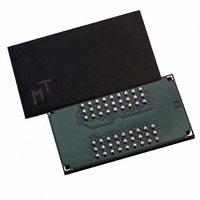
MT48H4M16LFB4-8 IT Micron Technology Inc, MT48H4M16LFB4-8 IT Datasheet - Page 29

MT48H4M16LFB4-8 IT
Manufacturer Part Number
MT48H4M16LFB4-8 IT
Description
IC SDRAM 64MBIT 125MHZ 54VFBGA
Manufacturer
Micron Technology Inc
Datasheet
1.MT48H4M16LFB4-10.pdf
(54 pages)
Specifications of MT48H4M16LFB4-8 IT
Format - Memory
RAM
Memory Type
Mobile SDRAM
Memory Size
64M (4M x 16)
Speed
125MHz
Interface
Parallel
Voltage - Supply
1.7 V ~ 1.9 V
Operating Temperature
-40°C ~ 85°C
Package / Case
54-VFBGA
Lead Free Status / RoHS Status
Lead free / RoHS Compliant
10. For a READ without auto precharge interrupted by a READ (with or without auto precharge), the READ to bank m will
11. For a READ without auto precharge interrupted by a WRITE (with or without auto precharge), the WRITE to bank m will
12. For a WRITE without auto precharge interrupted by a READ (with or without auto precharge), the READ to bank m will
13. For a WRITE without auto precharge interrupted by a WRITE (with or without auto precharge), the WRITE to bank m
14. For a READ with auto precharge interrupted by a READ (with or without auto precharge), the READ to bank m will
15. For a READ with auto precharge interrupted by a WRITE (with or without auto precharge), the WRITE to bank m will
16. For a WRITE with auto precharge interrupted by a READ (with or without auto precharge), the READ to bank m will
17. For a WRITE with auto precharge interrupted by a WRITE (with or without auto precharge), the WRITE to bank m will
pdf: 09005aef80a63953, source: 09005aef808a7edc
Y25L_64Mb_2.fm - Rev. E 11/04 EN
7. READs or WRITEs to bank m listed in the Command (Action) column include READs or WRITEs with auto precharge
8. CONCURRENT AUTO PRECHARGE: Bank n will initiate the auto precharge command when its burst has been interrupted
9. Burst in bank n continues as initiated.
enabled and READs or WRITEs with auto precharge disabled.
by bank m’s burst.
interrupt the READ on bank n, CAS latency later (Figure 10, Consecutive READ Bursts, on page 17).
interrupt the READ on bank n when registered (Figure 12, READ to WRITE, on page 18, and Figure 13, READ to WRITE
with Extra Clock Cycle, on page 18). DQM should be used one clock prior to the WRITE command to prevent bus conten-
tion.
interrupt the WRITE on bank n when registered (Figure 20, WRITE to READ, on page 21), with the data-out appearing
CAS latency later. The last valid WRITE to bank n will be data-in registered one clock prior to the READ to bank m.
will interrupt the WRITE on bank n when registered (Figure 18, WRITE to WRITE, on page 20). The last valid WRITE to
bank n will be data-in registered one clock prior to the READ to bank m.
interrupt the READ on bank n, CAS latency later (Figure 27, READ With Auto Precharge Interrupted by a READ, on
page 24). The PRECHARGE to bank n will begin when the READ to bank m is registered.
interrupt the READ on bank n when registered (Figure 28, READ With Auto Precharge Interrupted by a WRITE, on
page 24). DQM should be used two clocks prior to the WRITE command to prevent bus contention. The PRECHARGE to
bank n will begin when the WRITE to bank m is registered.
interrupt the WRITE on bank n when registered, with the data-out appearing CAS latency later (Figure 29, WRITE With
Auto Precharge Interrupted by a READ, on page 25). The PRECHARGE to bank n will begin after
begins when the READ to bank m is registered. The last valid WRITE bank n will be data-in registered one clock prior to
the READ to bank m.
interrupt the WRITE on bank n when registered. The PRECHARGE to bank n will begin after
begins when the WRITE to bank m is registered (Figure 30, WRITE With Auto Precharge Interrupted by a WRITE, on
page 25). The last valid WRITE to bank n will be data registered one clock to the WRITE to bank m.
29
Micron Technology, Inc., reserves the right to change products or specifications without notice.
MOBILE SDRAM
©2003 Micron Technology, Inc. All rights reserved.
t
WR is met, where
t
WR is met, where
64Mb: x16
t
WR
t
WR


