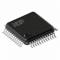
PCA9626B,118 NXP Semiconductors, PCA9626B,118 Datasheet - Page 23

PCA9626B,118
Manufacturer Part Number
PCA9626B,118
Description
IC LED DRIVER RGBA 48-LQFP
Manufacturer
NXP Semiconductors
Type
RGBA LED Driverr
Specifications of PCA9626B,118
Package / Case
48-LQFP
Topology
Open Drain, PWM
Number Of Outputs
24
Internal Driver
Yes
Type - Primary
Backlight, LED Blinker
Type - Secondary
RGBA
Frequency
1MHz
Voltage - Supply
2.3 V ~ 5.5 V
Voltage - Output
40V
Mounting Type
Surface Mount
Operating Temperature
-40°C ~ 85°C
Current - Output / Channel
100mA
Internal Switch(s)
Yes
Number Of Segments
24
Low Level Output Current
100000 uA (Min)
Operating Supply Voltage
2.3 V to 5.5 V
Maximum Supply Current
18000 uA
Maximum Power Dissipation
1800 mW
Maximum Operating Temperature
+ 85 C
Mounting Style
SMD/SMT
Minimum Operating Temperature
- 40 C
Lead Free Status / RoHS Status
Lead free / RoHS Compliant
Efficiency
-
Lead Free Status / Rohs Status
Lead free / RoHS Compliant
Other names
568-4774-2
Available stocks
Company
Part Number
Manufacturer
Quantity
Price
Company:
Part Number:
PCA9626B,118
Manufacturer:
NXP Semiconductors
Quantity:
10 000
Part Number:
PCA9626B,118
Manufacturer:
NXP/恩智浦
Quantity:
20 000
NXP Semiconductors
PCA9626_2
Product data sheet
7.3.8 SUBADR1 to SUBADR3, I
7.3.9 ALLCALLADR, LED All Call I
Table 13.
Legend: * default value.
Subaddresses are programmable through the I
E4h, E8h, and the device(s) will not acknowledge these addresses right after power-up
(the corresponding SUBx bit in MODE1 register is equal to 0).
Once subaddresses have been programmed to their right values, SUBx bits need to be
set to logic 1 in order to have the device acknowledging these addresses (MODE1
register).
Only the 7 MSBs representing the I
register is a read-only bit (0).
When SUBx is set to logic 1, the corresponding I
either an I
Table 14.
Legend: * default value.
The LED All Call I
at the same time (ALLCALL bit in register MODE1 must be equal to logic 1 (power-up
default state)). This address is programmable through the I
either an I
as a Sub Call.
Only the 7 MSBs representing the All Call I
ALLCALLADR register is a read-only bit (0).
If ALLCALL bit = 0, the device does not acknowledge the address programmed in register
ALLCALLADR.
Address
23h
24h
25h
Address
26h
2
2
Register
SUBADR1
SUBADR2
SUBADR3
Register
ALLCALLADR
SUBADR1 to SUBADR3 - I
bit description
ALLCALLADR - LED All Call I
description
C-bus read or write sequence.
C-bus read or write sequence. The register address can also be programmed
2
C-bus address allows all the PCA9626s on the bus to be programmed
Rev. 02 — 31 August 2009
Bit
7:1
0
7:1
0
7:1
0
Bit
7:1
0
2
C-bus subaddress 1 to 3
Symbol
A1[7:1]
A1[0]
A2[7:1]
A2[0]
A3[7:1]
A3[0]
Symbol
AC[7:1]
AC[0]
2
C-bus address
2
2
C-bus subaddress are valid. The LSB in SUBADRx
C-bus subaddress registers 0 to 3 (address 23h to 25h)
2
C-bus address register (address 26h) bit
Access Value
R/W
R only
R/W
R only
R/W
R only
2
24-bit Fm+ I
Access Value
R/W
R only
C-bus address are valid. The LSB in
2
C-bus. Default power-up values are E2h,
2
C-bus subaddress can be used during
1110 001*
0*
1110 010*
0*
1110 100*
0*
1110 000*
0*
2
C-bus 100 mA 40 V LED driver
2
C-bus and can be used during
Description
I
reserved
I
reserved
I
reserved
2
2
2
Description
ALLCALL I
address register
reserved
C-bus subaddress 1
C-bus subaddress 2
C-bus subaddress 3
PCA9626
© NXP B.V. 2009. All rights reserved.
2
C-bus
23 of 47


