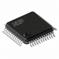
PCA9626B,118 NXP Semiconductors, PCA9626B,118 Datasheet - Page 38

PCA9626B,118
Manufacturer Part Number
PCA9626B,118
Description
IC LED DRIVER RGBA 48-LQFP
Manufacturer
NXP Semiconductors
Type
RGBA LED Driverr
Specifications of PCA9626B,118
Package / Case
48-LQFP
Topology
Open Drain, PWM
Number Of Outputs
24
Internal Driver
Yes
Type - Primary
Backlight, LED Blinker
Type - Secondary
RGBA
Frequency
1MHz
Voltage - Supply
2.3 V ~ 5.5 V
Voltage - Output
40V
Mounting Type
Surface Mount
Operating Temperature
-40°C ~ 85°C
Current - Output / Channel
100mA
Internal Switch(s)
Yes
Number Of Segments
24
Low Level Output Current
100000 uA (Min)
Operating Supply Voltage
2.3 V to 5.5 V
Maximum Supply Current
18000 uA
Maximum Power Dissipation
1800 mW
Maximum Operating Temperature
+ 85 C
Mounting Style
SMD/SMT
Minimum Operating Temperature
- 40 C
Lead Free Status / RoHS Status
Lead free / RoHS Compliant
Efficiency
-
Lead Free Status / Rohs Status
Lead free / RoHS Compliant
Other names
568-4774-2
Available stocks
Company
Part Number
Manufacturer
Quantity
Price
Company:
Part Number:
PCA9626B,118
Manufacturer:
NXP Semiconductors
Quantity:
10 000
Part Number:
PCA9626B,118
Manufacturer:
NXP/恩智浦
Quantity:
20 000
NXP Semiconductors
Table 19.
[1]
[2]
[3]
[4]
[5]
[6]
PCA9626_2
Product data sheet
Symbol Parameter
Output port timing
t
t
d(SCL-Q)
d(SDA-Q)
Fig 18. Definition of timing
t
t
A master device must internally provide a hold time of at least 300 ns for the SDA signal (refer to the V
bridge the undefined region of SCL’s falling edge.
The maximum t
250 ns. This allows series protection resistors to be connected between the SDA and the SCL pins and the SDA/SCL bus lines without
exceeding the maximum specified t
C
Input filters on the SDA and SCL inputs suppress noise spikes less than 50 ns.
VD;ACK
VD;DAT
b
SDA
SCL
= total capacitance of one bus line in pF.
= minimum time for SDA data out to be valid following SCL LOW.
delay time from SCL
to data output
delay time from SDA
to data output
= time for Acknowledgement signal from SCL LOW to SDA (out) LOW.
Dynamic characteristics
P
t
BUF
f
for the SDA and SCL bus lines is specified at 300 ns. The maximum fall time (t
S
t
HD;STA
t
LOW
Conditions
SCL to LEDn;
MODE2[3] = 1;
outputs change on
ACK
SDA to LEDn;
MODE2[3] = 0;
outputs change on
STOP condition
f
.
…continued
t
t
r
HD;DAT
Rev. 02 — 31 August 2009
t
HIGH
t
f
t
SU;DAT
Standard-mod
Min
e I
-
-
2
C-bus
24-bit Fm+ I
Max
-
-
Sr
t
SU;STA
Fast-mode
Min
t
HD;STA
I
-
-
2
2
f
C-bus
C-bus 100 mA 40 V LED driver
) for the SDA output stage is specified at
IL
Max
of the SCL signal) in order to
-
-
t
SP
t
SU;STO
PCA9626
Plus I
Min
Fast-mode
© NXP B.V. 2009. All rights reserved.
-
-
2
C-bus
002aaa986
Max
450
450
P
38 of 47
Unit
ns
ns


