MCZ33883EG Freescale Semiconductor, MCZ33883EG Datasheet - Page 10
MCZ33883EG
Manufacturer Part Number
MCZ33883EG
Description
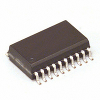
IC PRE-DRIVER FULL BRIDGE 20SOIC
Manufacturer
Freescale Semiconductor
Type
High Side/Low Sider
Datasheet
1.MCZ33883EGR2.pdf
(21 pages)
Specifications of MCZ33883EG
Configuration
H Bridge
Input Type
Non-Inverting
Delay Time
200ns
Current - Peak
2A
Number Of Configurations
1
Number Of Outputs
4
Voltage - Supply
5.5 V ~ 55 V
Operating Temperature
-40°C ~ 125°C
Mounting Type
Surface Mount
Package / Case
20-SOIC (7.5mm Width)
Rise Time
180 ns
Fall Time
180 ns
Supply Voltage (min)
5.5 V
Supply Current
2.2 mA
Maximum Power Dissipation
1250 mW
Maximum Operating Temperature
+ 125 C
Mounting Style
SMD/SMT
Bridge Type
H Bridge
Minimum Operating Temperature
- 40 C
Number Of Drivers
4
Lead Free Status / RoHS Status
Lead free / RoHS Compliant
High Side Voltage - Max (bootstrap)
-
Lead Free Status / Rohs Status
Lead free / RoHS Compliant
Available stocks
Company
Part Number
Manufacturer
Quantity
Price

Part Number:
MCZ33883EG
Manufacturer:
FREESCALE
Quantity:
20 000
Company:
Part Number:
MCZ33883EGR2
Manufacturer:
FREESCALE
Quantity:
1 490
Part Number:
MCZ33883EGR2
Manufacturer:
FREESCALE
Quantity:
20 000


driver) with integrated charge pump and independent high-
and low-side driver channels. It has the capability to drive
SUPPLY VOLTAGE TERMINALS (VCC AND VCC2)
to the device. V
the charge pump. V
can be connected together or independent with different
voltage values. The device can operate with V
and V
and overvoltage (OV) shutdown. If one of the supply voltage
drops below the undervoltage threshold or rises above the
overvoltage threshold, the gate outputs are switched LOW in
order to switch off the external MOSFETs. When the supply
returns to a level that is above the UV threshold or below the
OV threshold, the device resumes normal operation
according to the established condition of the input terminals.
INPUT HIGH- AND LOW-SIDE TERMINALS
(IN_HS1, IN_HS2, AND IN_LS1, IN_LS2)
terminals used to control the gate outputs. These terminals
are 5.0 V CMOS-compatible inputs with hysteresis. IN_HSn
and IN_LSn independently control GATE_HSn and
GATE_LSn, respectively.
terminal. There is no internal circuit to prevent the external
high-side and low-side MOSFETs from conducting at the
same time.
SOURCE OUTPUT HIGH-SIDE TERMINALS
(SRC_HS1 AND SRC_HS2)
high-side MOSFETs. The external high-side MOSFETs are
controlled using the
GATE HIGH- AND LOW-SIDE TERMINALS
(GATE_HS1, GATE_HS2, AND GATE_LS1,
GATE_LS2)
of the external high- and low-side MOSFETs. The external
high- and low-side MOSFETs are controlled using the
IN_HSn and IN_LSn inputs.
10
33883
FUNCTIONAL DESCRIPTION
INTRODUCTION
The 33883 is an H-bridge gate driver (or full-bridge pre-
The VCC and VCC2 terminals are the power supply inputs
The VCC and VCC2 terminals have undervoltage (UV)
The IN_HSn and IN_LSn terminals are input control
During wake-up, the logic is supplied from the G_EN
The SRC_HSn terminals are the sources of the external
The GATE_HSn and GATE_LSn terminals are the gates
CC2
up to 28 V.
CC
is used for the output high-side drivers and
CC2
IN_HSn inputs.
is used for the linear regulation. They
FUNCTIONAL TERMINAL DESCRIPTION
FUNCTIONAL DESCRIPTION
CC
up to 55 V
INTRODUCTION
large gate-charge MOSFETs and supports high PWM
frequency. In sleep mode its supply current is very low.
GLOBAL ENABLE (G_EN)
mode. When the G_EN terminal voltage is a logic LOW state,
the device is in sleep mode. The device is enabled and fully
operational when the G_EN terminal voltage is logic HIGH,
typically 5.0 V.
CHARGE PUMP OUT (CP_OUT)
reservoir capacitor for the charge pump.
CHARGE PUMP CAPACITOR TERMINALS
(C1 AND C2)
capacitor for the charge pump.
LINEAR REGULATOR OUTPUT (LR_OUT)
regulator. It is used to connect an external capacitor.
GROUND TERMINALS
(GND_A, GND1 AND GND2)
They should be connected together with a very low
impedance connection.
The G_EN terminal is used to place the device in a sleep
The CP_OUT terminal is used to connect an external
The C1 and C2 terminals are used to connect an external
The LR_OUT terminal is the output of the internal
These terminals are the ground terminals of the device.
Analog Integrated Circuit Device Data
Freescale Semiconductor
Related parts for MCZ33883EG
Image
Part Number
Description
Manufacturer
Datasheet
Request
R

Part Number:
Description:
Manufacturer:
Freescale Semiconductor, Inc
Datasheet:
Part Number:
Description:
Manufacturer:
Freescale Semiconductor, Inc
Datasheet:
Part Number:
Description:
Manufacturer:
Freescale Semiconductor, Inc
Datasheet:
Part Number:
Description:
Manufacturer:
Freescale Semiconductor, Inc
Datasheet:
Part Number:
Description:
Manufacturer:
Freescale Semiconductor, Inc
Datasheet:
Part Number:
Description:
Manufacturer:
Freescale Semiconductor, Inc
Datasheet:
Part Number:
Description:
Manufacturer:
Freescale Semiconductor, Inc
Datasheet:
Part Number:
Description:
Manufacturer:
Freescale Semiconductor, Inc
Datasheet:
Part Number:
Description:
Manufacturer:
Freescale Semiconductor, Inc
Datasheet:
Part Number:
Description:
Manufacturer:
Freescale Semiconductor, Inc
Datasheet:
Part Number:
Description:
Manufacturer:
Freescale Semiconductor, Inc
Datasheet:
Part Number:
Description:
Manufacturer:
Freescale Semiconductor, Inc
Datasheet:
Part Number:
Description:
Manufacturer:
Freescale Semiconductor, Inc
Datasheet:
Part Number:
Description:
Manufacturer:
Freescale Semiconductor, Inc
Datasheet:
Part Number:
Description:
Manufacturer:
Freescale Semiconductor, Inc
Datasheet: