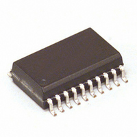
MCZ33883EG Freescale Semiconductor, MCZ33883EG Datasheet - Page 7

MCZ33883EG
Manufacturer Part Number
MCZ33883EG
Description
IC PRE-DRIVER FULL BRIDGE 20SOIC
Manufacturer
Freescale Semiconductor
Type
High Side/Low Sider
Datasheet
1.MCZ33883EGR2.pdf
(21 pages)
Specifications of MCZ33883EG
Configuration
H Bridge
Input Type
Non-Inverting
Delay Time
200ns
Current - Peak
2A
Number Of Configurations
1
Number Of Outputs
4
Voltage - Supply
5.5 V ~ 55 V
Operating Temperature
-40°C ~ 125°C
Mounting Type
Surface Mount
Package / Case
20-SOIC (7.5mm Width)
Rise Time
180 ns
Fall Time
180 ns
Supply Voltage (min)
5.5 V
Supply Current
2.2 mA
Maximum Power Dissipation
1250 mW
Maximum Operating Temperature
+ 125 C
Mounting Style
SMD/SMT
Bridge Type
H Bridge
Minimum Operating Temperature
- 40 C
Number Of Drivers
4
Lead Free Status / RoHS Status
Lead free / RoHS Compliant
High Side Voltage - Max (bootstrap)
-
Lead Free Status / Rohs Status
Lead free / RoHS Compliant
Available stocks
Company
Part Number
Manufacturer
Quantity
Price
Part Number:
MCZ33883EG
Manufacturer:
FREESCALE
Quantity:
20 000
Company:
Part Number:
MCZ33883EGR2
Manufacturer:
FREESCALE
Quantity:
1 490
Part Number:
MCZ33883EGR2
Manufacturer:
FREESCALE
Quantity:
20 000
Table 3. Static Electrical Characteristics (continued)
values noted reflect the approximate parameter means at T
Analog Integrated Circuit Device Data
Freescale Semiconductor
SUPPLY VOLTAGE
OUTPUT
Notes
Quiescent VCC Supply Current
Operating VCC Supply Current
Additional Operating V
Active
Quiescent VCC2 Supply Current
Operating VCC2 Supply Current
Additional Operating VCC2 Supply Current for Each Logic Input Terminal
Active
Undervoltage Shutdown VCC
Undervoltage Shutdown VCC2
Overvoltage Shutdown VCC
Overvoltage Shutdown VCC2
Output Sink Resistance (Turned Off)
Output Source Resistance (Turned On)
Charge Current of the External High-Side MOSFET Through GATE_HSn
Terminal
Maximum Voltage (V
Characteristics noted under conditions V
6.
7.
8.
9.
V
V
V
V
V
V
V
V
V
V
I discharge LSS = 50 mA , V
I charge HSS = 50 mA, V
INH = Logic 1, I
G_EN
G_EN
CC
CC
CC
G_EN
G_EN
CC
CC
CC
Logic input terminal inactive (high impedance).
High-frequency PWM-ing (
remain within the package power handling rating.
The device may exhibit predictable behavior between 4.0 V and 5.5 V.
See
= 55 V and V
= 12 V and V
= 55 V and V
= 55 V and V
= 12 V and V
= 55 V and V
(9)
= 0 V and V
= 0 V and V
= 0 V and V
= 0 V and V
Figure
5, page 12, for a description of charge current.
S
max = 5.0 mA
GATE_HS
CC2
CC2
CC2
CC2
CC2
CC2
CC
CC
CC
CC
CC
= 55 V
= 12 V
= 28 V
= 12 V
Supply Current for Each Logic Input Terminal
= 28 V
= 28 V
= 12 V
= 28 V
= 12 V
= 28 V
CP_OUT
Characteristic
SRC_HS
- V
(8)
(6)
(6)
»
(7)
(7)
SRC_HS
20 kHz) of the logic inputs will result in greater power dissipation within the device. Care must be taken to
= 20 V
= 0 V
)
(8)
(8)
CC
= 12 V, V
CC2
A
= 12 V, C
= 25°C under nominal conditions unless otherwise noted.
CP
I
IV
CHARGE HSS
IV
IV
= 33 nF, G_EN = 4.5 V unless otherwise noted. Typical
IV
IV
CC2SLEEP
Symbol
IV
CCSLEEP
VMAX
CC2LOG
CCLOG
CC2OP
UV2
OV2
R
R
CCOP
OV
UV
DS
DS
STATIC ELECTRICAL CHARACTERISTICS
29.5
Min
4.0
4.0
57
–
–
–
–
–
–
–
–
–
–
–
–
–
–
ELECTRICAL CHARACTERISTICS
Typ
100
2.2
0.7
5.0
5.0
61
31
–
–
–
–
–
–
–
–
–
–
–
Max
200
5.0
5.0
5.0
9.0
5.0
5.5
5.5
10
10
12
65
35
22
22
18
–
–
Unit
mA
mA
mA
mA
mA
µA
µA
33883
V
V
V
V
Ω
Ω
V
7


