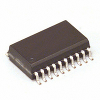
MCZ33883EG Freescale Semiconductor, MCZ33883EG Datasheet - Page 14

MCZ33883EG
Manufacturer Part Number
MCZ33883EG
Description
IC PRE-DRIVER FULL BRIDGE 20SOIC
Manufacturer
Freescale Semiconductor
Type
High Side/Low Sider
Datasheet
1.MCZ33883EGR2.pdf
(21 pages)
Specifications of MCZ33883EG
Configuration
H Bridge
Input Type
Non-Inverting
Delay Time
200ns
Current - Peak
2A
Number Of Configurations
1
Number Of Outputs
4
Voltage - Supply
5.5 V ~ 55 V
Operating Temperature
-40°C ~ 125°C
Mounting Type
Surface Mount
Package / Case
20-SOIC (7.5mm Width)
Rise Time
180 ns
Fall Time
180 ns
Supply Voltage (min)
5.5 V
Supply Current
2.2 mA
Maximum Power Dissipation
1250 mW
Maximum Operating Temperature
+ 125 C
Mounting Style
SMD/SMT
Bridge Type
H Bridge
Minimum Operating Temperature
- 40 C
Number Of Drivers
4
Lead Free Status / RoHS Status
Lead free / RoHS Compliant
High Side Voltage - Max (bootstrap)
-
Lead Free Status / Rohs Status
Lead free / RoHS Compliant
Available stocks
Company
Part Number
Manufacturer
Quantity
Price
Part Number:
MCZ33883EG
Manufacturer:
FREESCALE
Quantity:
20 000
Company:
Part Number:
MCZ33883EGR2
Manufacturer:
FREESCALE
Quantity:
1 490
Part Number:
MCZ33883EGR2
Manufacturer:
FREESCALE
Quantity:
20 000
LOW-DROP LINEAR REGULATOR
exceeds 15.0 V, the output is limited to 14.5 V (typical).
logic section of the driver, the V
the +14.5 V for the charge pump, which generates the
CP_OUT The low-drop linear regulator provides 4.0 mA
average current per driver stage.
16 mA — 8.0 mA for the high side and 8.0 mA for the low
side.
a frequency of 100 kHz is:
In a full-bridge application only one high side and one low
side switches on or off at the same time.
CHARGE PUMP
voltage (CP_OUT), buffered at C
charge pump basic circuit without load.
charged through D2 until its voltage reaches V
the oscillator is in high state (2), C
in C
is V
is about 330 kHz.
EXTERNAL CAPACITORS CHOICE
regulator are necessary to supply high peak current
absorbed during switching.
gate driver. Transistors Tosc1 and Tosc2 are the oscillator-
switching MOSFETs. When Tosc1 is on, the oscillator is at
low level. When Tosc2 is on, the oscillator is at high level. The
14
33883
FUNCTIONAL DEVICE OPERATION
OPERATIONAL MODES
The low-drop linear regulator is supplied by V
The low-drop linear regulator provides the 5.0 V for the
In case of the full bridge, that means approximately
Note: The average current required to switch a gate with
The charge pump generates the high-side driver supply
When the oscillator is in low state [(1) in
External capacitors on the charge pump and on the linear
Figure 9
V
V
cc
Osc.
CP_OUT,
LR_OUT
LR_OUT
OSC.
+ V
I
CP
LR_OUT
Figure 8. Charge Pump Basic Circuit
represents a simplified circuitry of the high-side
and final voltage of the charge pump, V
= Q
C1
g
- 2V
* f
PWM
Ccp
C
D
CP
. The frequency of the 33883 oscillator
(2)
= 80 nC * 100 kHz = 8.0 mA
(1)
gs_ls
CP_OUT
CP
A
C2
buffered at LR_OUT, and
D1
D2
is discharged though D1
D2
D1
.
Figure 8
Figure
CC
CC2
- V
shows the
C
CP_OUT
V
V
8], C
Ccp_out
Vbat
D2
CP_OUT
CP_OUT
. If V
CC
CP_OUT
. When
CP
CC2
is
,
capacitor C
MOSFET through HSS during turn-on (3).
V
LR_OUT
V
pins
Terminals
LR-OUT
HSS
LSS
T1
T2
CP_OUT
Tosc2
Tosc1
Tosc2
Tosc1
Figure 9. High-Side Gate Driver
C1
C1
provides peak current to the high-side
Ccp
C
Analog Integrated Circuit Device Data
CP
GATE_HS
SRC_HS
GATE_HS
C2
C2
SRC_HS
Rg
Rg
Freescale Semiconductor
V
CP_OUT
Vcc
(3)
CC
CP_out
D1
D1
D2
D2
High-Side
MOSFET
Low-Side
MOSFET
LS
MOSFET
C
Ccp_out
HS
MOSFET
CP_OUT


