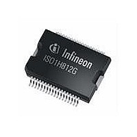
ISO1H812G Infineon Technologies, ISO1H812G Datasheet - Page 10

ISO1H812G
Manufacturer Part Number
ISO1H812G
Description
IC SWITCH HISIDE 8CH DSO-36
Manufacturer
Infineon Technologies
Type
High Sider
Series
ISOFACE™r
Datasheet
1.ISO1H812G.pdf
(22 pages)
Specifications of ISO1H812G
Package / Case
DSO-36
Input Type
Serial
Number Of Outputs
8
On-state Resistance
150 mOhm
Current - Output / Channel
700mA
Current - Peak Output
1.4A
Voltage - Supply
11 V ~ 35 V
Operating Temperature
-25°C ~ 125°C
Mounting Type
Surface Mount
Product
Driver ICs - Various
Supply Voltage (max)
6.5 V
Supply Voltage (min)
- 0.5 V
Maximum Power Dissipation
3.3 W
Maximum Operating Temperature
Internally Limited
Mounting Style
SMD/SMT
Minimum Operating Temperature
- 25 C
Output Current
0.625 A
Lead Free Status / RoHS Status
Lead free / RoHS Compliant
Lead Free Status / RoHS Status
Lead free / RoHS Compliant, Lead free / RoHS Compliant
Other names
SP000413800
Available stocks
Company
Part Number
Manufacturer
Quantity
Price
Company:
Part Number:
ISO1H812G
Manufacturer:
INTERSIL
Quantity:
101
more ICs is needed. All ICs share the same clock and
chip select port of the SPI master. That is all ICs are
active and addressed simultaneously. The data out of
the µC is connected to the SI of the first IC in the line.
Each SO of an IC is connected to the SI of the next IC
in the line.
Figure 10
The µC feeds to data bits into the SI of IC1 (first IC in
the chain). The bits coming from the SO of IC1 are
directly shifted into the SI of the next IC. As long as the
chip select is inactive (logic high) all the IC SPIs ignore
the clock (SCLK) and input signals (SI) and all outputs
(SO) are in tristate. As long as the chip select is active
the SPI register works as a simple shift register. With
each clock signal one input is shifted into the SPI
register (SI), each bit in the shift register moves one
position further within the register, and the last bit in the
SPI shift register is shifted out of SO. This continous as
long as the chip select is active (logic low) and clock
signals are applied. The data is then only taken over to
the output buffers of each IC when the CS signal
changes to high from low and recognized as valid data
by the internal modulo counter.
3.6
There is a failure detection unit integrated to ensure
also a stable functionality during the integrated
coreless transformer transmission. This unit decides
Datasheet
µC
SPI 1
Tx a1
Tx a2
Number of adressed ICs = n
Number of necessary control and data ports = 3
All ICs are adressed by the common chip select
CLK
SPI bus all ICs in a “daisy chain”
configuration
Transmission Failure Detection
IC1
ICn
SPI - Interface
SPI - Interface
SCLK
CS
SI
SO
SCLK
CS
SI
Output lines
Output lines
10
wether the transmitted data is valid or not. If four times
serial data coming from the internal registers is not
accepted the output stages are switched off until the
next valid data is received.
Functional Description
Version 2.2, 2009-07-01
ISOFACE
ISO1H812G
TM


