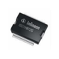
ISO1H812G Infineon Technologies, ISO1H812G Datasheet - Page 15

ISO1H812G
Manufacturer Part Number
ISO1H812G
Description
IC SWITCH HISIDE 8CH DSO-36
Manufacturer
Infineon Technologies
Type
High Sider
Series
ISOFACE™r
Datasheet
1.ISO1H812G.pdf
(22 pages)
Specifications of ISO1H812G
Package / Case
DSO-36
Input Type
Serial
Number Of Outputs
8
On-state Resistance
150 mOhm
Current - Output / Channel
700mA
Current - Peak Output
1.4A
Voltage - Supply
11 V ~ 35 V
Operating Temperature
-25°C ~ 125°C
Mounting Type
Surface Mount
Product
Driver ICs - Various
Supply Voltage (max)
6.5 V
Supply Voltage (min)
- 0.5 V
Maximum Power Dissipation
3.3 W
Maximum Operating Temperature
Internally Limited
Mounting Style
SMD/SMT
Minimum Operating Temperature
- 25 C
Output Current
0.625 A
Lead Free Status / RoHS Status
Lead free / RoHS Compliant
Lead Free Status / RoHS Status
Lead free / RoHS Compliant, Lead free / RoHS Compliant
Other names
SP000413800
Available stocks
Company
Part Number
Manufacturer
Quantity
Price
Company:
Part Number:
ISO1H812G
Manufacturer:
INTERSIL
Quantity:
101
4.5
Parameter
at T
unless otherwise specified
Initial peak short circuit current limit, each channel:
T
T
T
Repetitive short circuit current limit
T
Repetitive short circuit current limit
T
Output clamp (inductive load switch off)
at V
Overvoltage protection
Thermal overload trip temperature
Thermal hysteresis
1) Integrated protection functions are designed to prevent IC destruction under fault conditions described in the data sheet.
2) Higher operating temperature at normal function for each channel available
3) not subject to production test, specified by design
4.6
Parameter
at T
unless otherwise specified
Common diagnostic sink current
(overtemperature of any channel) T
Common diagnostic source current
Datasheet
j
j
j
j
j
= -25°C, V
= T
= T
= 25°C
= 125°C
Fault conditions are considered as “outside” normal operating range. Protection functions are not designed for continuos
repetitive operation.
j
j
OUT
= -25 ... 125°C, V
= -25 ... 125°C, V
jt
jt
(see timing diagrams)
(see timing diagrams)
= V
1)
bb
bb
Output Protection Functions
Diagnostic Characteristics at pin DIAG
- V
= 30V, t
ON(CL)
3)
bb
bb
m
=15...30V, V
=15...30V, V
= 700µs
four parallel channels:
four parallel channels:
two parallel channels:
two parallel channels:
2) 3)
3)
CC
CC
j
each channel:
= 135°C
=3.0...5.5V,
=3.0...5.5V,
3)
3)
3)
3)
Symbol
I
I
Symbol
I
I
I
V
V
T
diagsink
diagsource
L(SCp)
L(SCr)
L(SCr)
four times the current of one channel
jt
T
ON(CL)
bb(AZ)
jt
twice the current of one channel
15
min.
min.
135
0.7
---
---
47
47
---
---
---
Limit Values
Limit Values
typ.
typ.
100
1.4
1.1
1.1
1.1
1.1
53
---
---
10
---
---
max.
max.
1.9
---
60
---
---
---
---
---
---
5
Electrical Characteristics
Version 2.2, 2009-07-01
Unit Test Condition
Unit Test Condition
A
V
°C
K
mA V
µA
VCC
DIAGON
ISOFACE
ISO1H812G
< 0.25 x
TM


