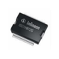
ISO1H812G Infineon Technologies, ISO1H812G Datasheet - Page 7

ISO1H812G
Manufacturer Part Number
ISO1H812G
Description
IC SWITCH HISIDE 8CH DSO-36
Manufacturer
Infineon Technologies
Type
High Sider
Series
ISOFACE™r
Datasheet
1.ISO1H812G.pdf
(22 pages)
Specifications of ISO1H812G
Package / Case
DSO-36
Input Type
Serial
Number Of Outputs
8
On-state Resistance
150 mOhm
Current - Output / Channel
700mA
Current - Peak Output
1.4A
Voltage - Supply
11 V ~ 35 V
Operating Temperature
-25°C ~ 125°C
Mounting Type
Surface Mount
Product
Driver ICs - Various
Supply Voltage (max)
6.5 V
Supply Voltage (min)
- 0.5 V
Maximum Power Dissipation
3.3 W
Maximum Operating Temperature
Internally Limited
Mounting Style
SMD/SMT
Minimum Operating Temperature
- 25 C
Output Current
0.625 A
Lead Free Status / RoHS Status
Lead free / RoHS Compliant
Lead Free Status / RoHS Status
Lead free / RoHS Compliant, Lead free / RoHS Compliant
Other names
SP000413800
Available stocks
Company
Part Number
Manufacturer
Quantity
Price
Company:
Part Number:
ISO1H812G
Manufacturer:
INTERSIL
Quantity:
101
3
3.1
The ISOface ISO1H812G includes 8 high-side power
switches that are controlled by means of the integrated
µC
OUT0...OUT7 are controlled by the data of the serial
input SI. The IC can replace 8 optocouplers and the 8
high-side switches in conventional I/O-Applications as
a galvanic isolation is implemented by means of the
integrated coreless transformer technology. The µC
compatible interfaces allow a direct connection to the
ports of a microcontroller without the need for other
components. Each of the 8 high-side power switches is
protected
overtemperature and against overvoltage by an active
zener clamp.
The diagnostic logic on the power chip recognizes the
overtemperature information of each power transistor
The information is send via the internal coreless
transformer to the pin DIAG at the input interface.
3.2
The IC contains 2 galvanic isolated voltage domains
that are independent from each other. The input
interface is supplied at VCC and the output stage is
supplied at Vbb. The different voltage domains can be
switched on at different time. The output stage is only
enabled once the input stage enters a stable state.
3.3
Each channel contains a high-side vertical power FET
that is protected by embedded protection functions.
The continuous current for each channel is 625mA (all
channels ON).
3.3.1
Each output is independently controlled by an output
latch and a common reset line via the pin DIS that
disables all eight outputs and reset the latches. Serial
data input (SI) is read on the rising edge of the serial
clock SCLK. A logic high input data bit turns the
respective output channel ON, a logic low data bit turns
it OFF. CS must be low whilst shifting all the serial data
into the device. A low-to-high transition of CS transfers
the serial data input bits to the output buffer.
Datasheet
compatible
Functional Description
Introduction
against
Power Supply
Output Stage
Output Stage Control
SPI
short
interface.
to
Vbb,
The
overload,
outputs
7
3.3.2
Each of the eight output stages has its own zener clamp
that causes a voltage limitation at the power transistor
when solenoid loads are switched off. V
clamped to 47V (min.).
Figure 3
Energy is stored in the load inductance during an
inductive load switch-off.
Figure 4
While demagnetizing the load inductance, the energy
dissipation in the DMOS is
with an approximate solution for R
E
E
E
L
AS
AS
=
=
=
1 2 L I
E
--------------- -
2 R
I
bb
L
V
bb
+
L
E
L
L
Power Transistor Overvoltage
Protection
Inductive and overvoltage output
clamp (each channel)
Inductive load switch-off energy
dissipation (each channel)
–
L
E
V
Dx
2
R
bb
=
+
V
E
V
ON CL
bb
GNDbb
ON CL
GNDbb
Vbb
Vz
OUTx
i
Functional Description
Version 2.2, 2009-07-01
L
t dt
ln
OUTx
L
E
Vbb
1
AS
> 0W:
+
Z
------------------------ -
L
V
I
ISOFACE
ISO1H812G
L
ON CL
R
L
L
V
R
ON
ON
E
L
Vbb
Load
E
E
L
R
is then
TM


