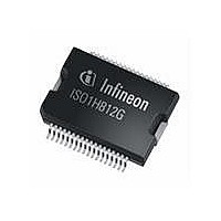
ISO1H812G Infineon Technologies, ISO1H812G Datasheet - Page 9

ISO1H812G
Manufacturer Part Number
ISO1H812G
Description
IC SWITCH HISIDE 8CH DSO-36
Manufacturer
Infineon Technologies
Type
High Sider
Series
ISOFACE™r
Datasheet
1.ISO1H812G.pdf
(22 pages)
Specifications of ISO1H812G
Package / Case
DSO-36
Input Type
Serial
Number Of Outputs
8
On-state Resistance
150 mOhm
Current - Output / Channel
700mA
Current - Peak Output
1.4A
Voltage - Supply
11 V ~ 35 V
Operating Temperature
-25°C ~ 125°C
Mounting Type
Surface Mount
Product
Driver ICs - Various
Supply Voltage (max)
6.5 V
Supply Voltage (min)
- 0.5 V
Maximum Power Dissipation
3.3 W
Maximum Operating Temperature
Internally Limited
Mounting Style
SMD/SMT
Minimum Operating Temperature
- 25 C
Output Current
0.625 A
Lead Free Status / RoHS Status
Lead free / RoHS Compliant
Lead Free Status / RoHS Status
Lead free / RoHS Compliant, Lead free / RoHS Compliant
Other names
SP000413800
Available stocks
Company
Part Number
Manufacturer
Quantity
Price
Company:
Part Number:
ISO1H812G
Manufacturer:
INTERSIL
Quantity:
101
3.5
The ISO1H812G contains a serial interface that can be
directly controlled by the microcontroller output ports.
3.5.1
the ISO1H812G by means of the CS pin. Whenever the
pin is in a logic low state, data can be transferred from
the µC.
CS High to low transition:
•Serial input data can be clocked in from then on
•SO changes from high impendance state to logic high
or low state corresponding to the SO bit-state
CS Low to high transition:
•Transfer of SI bits from shift register into output
buffers, if number of clock signals was an integer
multiple of 8
•SO changes from the SO bit-state to high impendance
state
To avoid any false clocking the serial input pin SCLK
should be logic high state during high-to-low transition
of CS. When CS is in a logic high state, any signals at
the SCLK and SI pins are ignored and SO is forced into
a high impedance state. The integrated modulo counter
that counts the number of clocks avoids the take over
of invalid commands caused by a spike on the clock
line or wrong number of clock cycles. A command is
only taken over if after the low-to-high transition of the
CS signal the number of counted clock cycles is an
integer multiple of 8.
SCLK - Serial clock. The system clock pin clocks the
internal shift register of the ISO1H812G. The serial
input (SI) accepts data into the input shift register on the
rising edge of SCLK while the serial output (SO) shifts
the output information out of the shift register on the
falling edge of the serial clock. It is essential that the
SCLK pin is in a logic high state whenever chip select
CS makes any transition. The number of clock pulses
will be counted during a chip select cycle. The received
data will only be accepted, if exactly an integer multiple
of 8 clock pulses were counted during CS is active.
Datasheet
CS - Chip select. The system microcontroller selects
Serial Interface
SPI Signal Description
9
SI - Serial input. Serial data bits are shifted in at this pin,
the most significant bit first. SI information is read in on
the rising edge of the SCLK. Input data is latched in the
shift register and then transferred to the control buffer
of the output stages.
SO - Serial output. SO is in a high impedance state until
the CS pin goes to a logic low state. The data of the
internal shift register are shifted out serially at this pin.
The most significant bit will appear at first. The further
bits will appear following the falling edge of SCLK.
3.5.2
3.5.2.1
Each IC with a SPI is controlled individually and
independently by an SPI master, as in a directional
point-to-point communication.The port requirements
for this topology are the greatest, because for each
controlled IC an individual SPI at the µC is needed
(SCLK, CS, SI). All ICs can be
simultaneously with the full SPI bandwidth.
Figure 9
3.5.2.2
Fig. 11 is called a daisy-chain. For this type of bus-
topology only one SPI interface of the µC for two or
The connection of different ICs and a µC as shown in
µC
SPI 1
SPI n
Tx a1
Tx a2
Tx n1
Tx n2
CLK
CLK
Number of adressed ICs = n
Number of necessary control and data ports = 3 n
Individual ICs are adressed by the chip select
SPI Bus Concepts
Independent Individual Control
Individual independent control of each
IC with SPI
Daisy-chain Configuration
Functional Description
Version 2.2, 2009-07-01
IC 1
IC n
SPI - Interface
SPI - Interface
SCLK
CS
SI
SO
SCLK
CS
SI
SO
ISOFACE
ISO1H812G
addressed
Output lines
Output lines
TM


