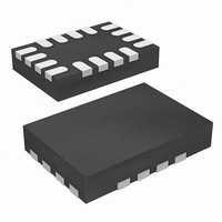
ISL62870HRUZ-T Intersil, ISL62870HRUZ-T Datasheet - Page 10

ISL62870HRUZ-T
Manufacturer Part Number
ISL62870HRUZ-T
Description
IC CTRLR VREG PWM DC/DC 16-TQFN
Manufacturer
Intersil
Datasheet
1.ISL62870HRUZ-T.pdf
(16 pages)
Specifications of ISL62870HRUZ-T
Pwm Type
Controller
Number Of Outputs
1
Frequency - Max
330kHz
Duty Cycle
100%
Voltage - Supply
3.3 V ~ 25 V
Buck
Yes
Boost
No
Flyback
No
Inverting
No
Doubler
No
Divider
No
Cuk
No
Isolated
No
Operating Temperature
-10°C ~ 100°C
Package / Case
16-UTQFN (16-µTQFN)
Frequency-max
330kHz
Lead Free Status / RoHS Status
Lead free / RoHS Compliant
Available stocks
Company
Part Number
Manufacturer
Quantity
Price
Company:
Part Number:
ISL62870HRUZ-T
Manufacturer:
M/A-COM
Quantity:
45
Part Number:
ISL62870HRUZ-T
Manufacturer:
INTERSIL
Quantity:
20 000
converter output voltage at the FB feedback pin follows the
voltage at the SREF pin. During soft-start, the regulator always
operates in CCM until the soft-start sequence is complete.
PGOOD Monitor
The PGOOD pin indicates when the converter is capable of
supplying regulated voltage. The PGOOD pin is an undefined
impedance if the VCC pin has not reached the rising POR
threshold V
POR threshold V
corresponds to a specific protective fault, thereby reducing
troubleshooting time and effort. Table 1 maps the pull-down
resistance of the PGOOD pin to the corresponding fault status
of the controller.
LGATE and UGATE MOSFET Gate-Drivers
The LGATE pin and UGATE pins are MOSFET driver
outputs. The LGATE pin drives the low-side MOSFET of the
converter while the UGATE pin drives the high-side
MOSFET of the converter.
The LGATE driver is optimized for low duty-cycle
applications where the low-side MOSFET experiences long
conduction times. In this environment, the low-side
MOSFETs require exceptionally low r
have large parasitic charges that conduct transient currents
within the devices in response to high dv/dt switching
present at the phase node. The drain-gate charge in
particular can conduct sufficient current through the driver
pull-down resistance that the V
exceeded and turned on. For this reason, the LGATE driver
has been designed with low pull-down resistance and high
sink current capability to ensure clamping the MOSFETs
gate voltage below V
Adaptive Shoot-Through Protection
Adaptive shoot-through protection prevents a gate-driver
output from turning on until the opposite gate-driver output
has fallen below approximately 1V. The dead-time shown in
Figure 7 is extended by the additional period that the falling
gate voltage remains above the 1V threshold. The high-side
gate-driver output voltage is measured across the UGATE
and PHASE pins while the low-side gate-driver output
voltage is measured across the LGATE and PGND pins. The
power for the LGATE gate-driver is sourced directly from the
PVCC pin. The power for the UGATE gate-driver is supplied
by a boot-strap capacitor connected across the BOOT and
PHASE pins. The capacitor is charged each time the phase
node voltage falls a diode drop below PVCC, such as when
the low-side MOSFET is turned on.
Soft-Start or Undervoltage
VCC Below POR
TABLE 1. PGOOD PULL-DOWN RESISTANCE
CONDITION
Overvoltage
Overcurrent
VCC_THR
VCC_THF
, or if the VCC pin is below the falling
GS(th)
. The PGOOD pull-down resistance
.
10
GS(th)
PGOOD RESISTANCE
DS(ON)
of the device can be
Undefined
95Ω
65Ω
35Ω
and tend to
ISL62870
Compensation Design
Figure 8 shows the recommended Type-II compensation
circuit. The FB pin is the inverting input of the error amplifier.
The COMP signal, the output of the error amplifier, is inside the
chip and unavailable to users. C
integrated inside the IC, connecting across the FB pin and the
COMP signal. R
compensator. The frequency domain transfer function is given
by Equation 12:
The LC output filter has a double pole at its resonant frequency
that causes rapid phase change. The R
IC makes the LC output filter resemble a first order system in
which the closed loop stability can be achieved with the
recommended Type-II compensation network. Intersil provides
a PC-based tool that can be used to calculate compensation
network component values and help simulate the loop
frequency response.
General Application Design Guide
This design guide is intended to provide a high-level
explanation of the steps necessary to design a single-phase
power converter. It is assumed that the reader is familiar with
G
COMP
COMP
FIGURE 7. GATE DRIVER ADAPTIVE SHOOT-THROUGH
FIGURE 8. COMPENSATION REFERENCE CIRCUIT
C
s ( )
INT
SREF
=
= 100pF
EA
-------------------------------------------------------------------------------------------------------------- -
s R
⋅
FB
1V
1V
+
-
1
FB
, R
+
FB
⋅
COMP
s
C
⋅
INT
(
R
FB
, C
⋅
UGATE
LGATE
(
1
R
+
R
COMP
COMP
R
+
OFS
INT
COMP
s R
⋅
is a 100pF capacitor
R
and C
COMP
FB
) C
3
C
⋅
modulator used in the
COMP
INT
COMP
⋅
C
1V
1V
COMP
form the Type-II
August 14, 2008
)
(EQ. 12)
VOUT
FN6708.0


