ISL6442IA Intersil, ISL6442IA Datasheet
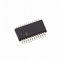
IC PWM BUCK VM 24QSOP

ISL6442IA

Manufacturer Part Number
ISL6442IA
Description
IC PWM BUCK VM 24QSOP
Manufacturer
Intersil
Datasheet

Specifications of ISL6442IA

Pwm Type
Voltage Mode
Number Of Outputs
3
Frequency - Max
2.85MHz
Duty Cycle
100%
Voltage - Supply
4.5 V ~ 24 V
Buck
Yes
Boost
No
Flyback
No
Inverting
No
Doubler
No
Divider
No
Cuk
No
Isolated
No
Operating Temperature
-40°C ~ 85°C
Package / Case
24-QSOP
Frequency-max
2.85MHz
Lead Free Status / RoHS Status
Contains lead / RoHS non-compliant

Available stocks

Company
Part Number
Manufacturer
Quantity
Price
Part Number:
ISL6442IAZ
Manufacturer:
Intersil
Quantity:
97
Part Number:
ISL6442IAZ
Manufacturer:
ST
Quantity:
6 267
Part Number:
ISL6442IAZ
Manufacturer:
INTERSIL
Quantity:
20 000
Part Number:
ISL6442IAZ-T
Manufacturer:
INTERSIL
Quantity:
20 000
Part Number:
ISL6442IAZ-TK
Manufacturer:
Intersil
Quantity:
6 000
Dual (180° Out-of-Phase) PWM and Linear
Controller
The ISL6442 is a high-performance, triple output controller
that provides a single high-frequency power solution
primarily for Broadband, DSL and Networking applications.
This device integrates complete control, monitoring and
protection functions for two synchronous buck PWM
controllers and one linear controller. Input voltage ripple and
total RMS input current is substantially reduced by
synchronized 180° out-of-phase operation of the two PWMs.
The two PWM buck converters provide simple voltage mode
control. The output voltage of the converters can be
precisely regulated to as low as 0.6V, with a maximum
tolerance of ±1.5% over temperature and line variations.
Programmable switching frequency up to 2.5MHz provides
fast transient response and small external components. The
linear controller provides a low-current output.
The ISL6442 has voltage-tracking capability. Each controller
has soft-start and independent enable functions combined
on a single pin. A capacitor from SS/EN to ground sets the
soft-start time; pulling SS/EN pin below 1V disables the
controller. Both outputs can soft-start into a pre-biased load.
The ISL6442 incorporates robust protection features. An
adjustable overcurrent protection circuit monitors the output
current by sensing the voltage drop across the upper
MOSFET r
protects the DC/DC converters from damage under over
load and short circuit conditions. A PGOOD signal is issued
when soft-start is complete and PWM outputs are within 10%
of their regulated values and the linear regulator output is
higher than 75% of its nominal value. Thermal shut-down
circuitry turns the device off if the IC temperature exceeds
+150°C.
Ordering Information
ISL6442IAZ*
*Add “-TK” suffix for tape and reel. Please refer to TB347 for details
on reel specifications.
NOTE: These Intersil Pb-free plastic packaged products employ
special Pb-free material sets, molding compounds/die attach
materials, and 100% matte tin plate plus anneal (e3 termination
finish, which is RoHS compliant and compatible with both SnPb and
Pb-free soldering operations). Intersil Pb-free products are MSL
classified at Pb-free peak reflow temperatures that meet or exceed
the Pb-free requirements of IPC/JEDEC J STD-020.
NUMBER
(Note)
PART
DS(ON)
ISL 6442IAZ
MARKING
PART
. Hiccup mode overcurrent operation
RANGE (°C)
®
-40 to +85
TEMP.
1
Data Sheet
24 Ld QSOP M24.15
PACKAGE
(Pb-free)
DWG. #
1-888-INTERSIL or 1-888-468-3774
PKG.
CAUTION: These devices are sensitive to electrostatic discharge; follow proper IC Handling Procedures.
Features
• 4.5V to 5.5V or 5.5V to 24V Input Voltage Range
• ±1.5% PWM Switcher Reference Accuracy Over Line and
• Three Programmable Power Output Voltages
• Programmable Switching Frequency from 300kHz to 2.5MHz
• Fast Transient Response
• Extensive Circuit Protection Functions
• Externally Adjustable Soft-Start Time
• PGOOD Output with Delay
• 24 Ld QSOP
• Pb-Free (RoHS Compliant)
Applications
• Complete 1 Chip Solution for DSL Modems/Routers
• DSP, ASIC, and FPGA Point of Load Regulation
• ADSL, Broadband and Networking Applications
Pinout
Temperature
- Two PWM Controllers with Out-of-Phase Operation
- Voltage-Mode PWM Control
- One Linear Controller
- High-Bandwidth Error Amplifier
- Overvoltage, Undervoltage, and Overtemperature
- Programmable Overcurrent Limit with Hiccup Mode
- Lossless Current Sensing (No Sense Resistor Needed)
- Independent Enable Control
- Voltage Tracking Capability
- Able to Soft-Start into a Pre-Biased Load
Operation
October 31, 2008
All other trademarks mentioned are the property of their respective owners.
|
Intersil (and design) is a registered trademark of Intersil Americas Inc.
SS1/EN1
SS2/EN2
OCSET1
OCSET2
COMP1
COMP2
SGND
LCDR
LCFB
Copyright Intersil Americas Inc. 2006, 2008. All Rights Reserved
FB1
FB2
RT
10
11
12
1
2
3
4
5
6
7
8
9
(24 LD QSOP)
TOP VIEW
ISL6442
24
23
22
21
20
19
18
17
16
15
14
13
VIN
BOOT1
UGATE1
PHASE1
LGATE1
VCC
PGND
LGATE2
PHASE2
UGATE2
BOOT2
PGOOD
ISL6442
FN9204.2

Related parts for ISL6442IA

ISL6442IA Summary of contents

Page 1

... NUMBER PART TEMP. (Note) MARKING RANGE (°C) ISL6442IAZ* ISL 6442IAZ -40 to +85 *Add “-TK” suffix for tape and reel. Please refer to TB347 for details on reel specifications. NOTE: These Intersil Pb-free plastic packaged products employ special Pb-free material sets, molding compounds/die attach ...

Page 2

Block Diagram REFERENCE BIAS CURRENT 30µA 100µA 0.6V COMP1 FB1 0.6V VCC5 VCC5 30µA 30µA SS1/EN1 SS2/EN2 0.6V FB2 COMP2 RT PGOOD SGND 2 ISL6442 VCC VCC POWER ON 5V LINEAR RESET REGULATOR AND CONTROL FAULT1 UVP1 OVP1 PG1 EN1 ...

Page 3

Typical Application Schematics VOLTAGE INPUTS REQUIRED VIN (4.5V TO 24V) = VIN1 = VIN2 VCC (5V; INTERNAL IF VIN > 5.6V) VIN3 (≤ VCC) FOR LINEAR TYPE3 COMPENSATION SHOWN C 102 R C 102 R 101 VOUT1 R C 103 ...

Page 4

... Maximum Junction Temperature (Plastic Package).-55°C to +150°C Maximum Storage Temperature Range . . . . . . . . . .-65°C to +150°C Temperature Range . . . . . . . . . . . . . . . . . . . . . . . . . .-40°C to +85°C Pb-Free Reflow Profile .see link below http://www.intersil.com/pbfree/Pb-FreeReflow.asp Recommended Operating Conditions VCC Supply Voltage . . . . . . . . . . . . . . . . . . . . . . . . . . . . . .5V ±10% VIN Supply Voltage . . . . . . . . . . . . . . . . . . . . . . . . . . . . 5.5V to 24V TEST CONDITIONS VIN = 5.5V or 12V ...

Page 5

Electrical Specifications Operating Conditions Unless Otherwise Noted: VIN = 12V values are at +25°C. Parameters with MIN and/or MAX limits are 100% tested at +25°C, unless otherwise specified. Temperature limits established by characterization and are not production tested. ...

Page 6

Electrical Specifications Operating Conditions Unless Otherwise Noted: VIN = 12V values are at +25°C. Parameters with MIN and/or MAX limits are 100% tested at +25°C, unless otherwise specified. Temperature limits established by characterization and are not production tested. ...

Page 7

Pin Descriptions BOOT1, 2 (Pins 23, 14) - These pins power the upper MOSFET drivers of each PWM converter. The anode of the each internal bootstrap diode is connected to the VCC pin. The cathode of the bootstrap diode is ...

Page 8

Then both 30µA current sources will start charging up both capacitors in parallel. Once the voltage on both of these pins is above 1.0V, this internal switch is turned off and each 30µA internal current source charges its corresponding ...

Page 9

Figure 8 shows pre-biased outputs before soft-start. The solid blue curve shows no pre-bias; the output starts ramping from GND. The magenta dotted line shows the output pre-biased to a voltage less than the final output. The FETs don’t turn ...

Page 10

RT (kΩ) FIGURE 10. FREQUENCY vs RT RESISTOR Output Regulation Figure 11 shows the generic feedback resistor circuit for any of the three V ’s; the ...

Page 11

UVP - (Function independent for both PWM). If the voltage on the FB pin falls to 82% (typical) of the reference voltage for 8 consecutive PWM cycles, then the circuit enters into soft-start hiccup mode. This mode is identical to ...

Page 12

High frequency decoupling capacitors should be placed as close to the power pins of the load as physically possible. Be careful not to add inductance in the circuit board wiring that could cancel the usefulness of these low inductance components. ...

Page 13

COMP - FB + E/A VREF OSCILLATOR V OSC PWM CIRCUIT UGATE HALF-BRIDGE DRIVE PHASE LGATE ISL6442 EXTERNAL CIRCUIT FIGURE 14. VOLTAGE-MODE BUCK CONVERTER COMPENSATION DESIGN The modulator transfer function is the small-signal transfer function of V ...

Page 14

COMPENSATION BREAK FREQUENCY EQUATIONS 1 F ------------------------------- - = ⋅ ⋅ Z1 2π -------------------------------------------------- - F = ⋅ ⋅ Z2 2π ---------------------------------------------- - = ⋅ ⋅ ...

Page 15

Q300 R307 LCDR R300 C300 LCFB R301 R302 FIGURE 16. LINEAR COMPENSATION COMPONENTS Strategy 1. The output capacitor of the linear regulator circuit must be chosen such that the ESR Zero is less than 200kHz: < F 200kHz Z1 2. ...

Page 16

... Accordingly, the reader is cautioned to verify that data sheets are current before placing orders. Information furnished by Intersil is believed to be accurate and reliable. However, no responsibility is assumed by Intersil or its subsidiaries for its use; nor for any infringements of patents or other rights of third parties which may result from its use ...

Related keywords