ISL6442IA Intersil, ISL6442IA Datasheet - Page 7
ISL6442IA
Manufacturer Part Number
ISL6442IA
Description
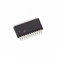
IC PWM BUCK VM 24QSOP
Manufacturer
Intersil
Datasheet
1.ISL6442IAZ-TK.pdf
(16 pages)
Specifications of ISL6442IA
Pwm Type
Voltage Mode
Number Of Outputs
3
Frequency - Max
2.85MHz
Duty Cycle
100%
Voltage - Supply
4.5 V ~ 24 V
Buck
Yes
Boost
No
Flyback
No
Inverting
No
Doubler
No
Divider
No
Cuk
No
Isolated
No
Operating Temperature
-40°C ~ 85°C
Package / Case
24-QSOP
Frequency-max
2.85MHz
Lead Free Status / RoHS Status
Contains lead / RoHS non-compliant
Available stocks
Company
Part Number
Manufacturer
Quantity
Price
Company:

Part Number:
ISL6442IAZ
Manufacturer:
Intersil
Quantity:
97
Company:
Part Number:
ISL6442IAZ
Manufacturer:
ST
Quantity:
6 267
Part Number:
ISL6442IAZ
Manufacturer:
INTERSIL
Quantity:
20 000
Part Number:
ISL6442IAZ-T
Manufacturer:
INTERSIL
Quantity:
20 000
Company:
Part Number:
ISL6442IAZ-TK
Manufacturer:
Intersil
Quantity:
6 000


Pin Descriptions
BOOT1, 2 (Pins 23, 14) - These pins power the upper
MOSFET drivers of each PWM converter. The anode of the
each internal bootstrap diode is connected to the VCC pin.
The cathode of the bootstrap diode is connected to this pin,
which should also connect to the bootstrap capacitor.
UGATE1, 2 (Pins 22, 15) - These pins provide the gate
drive for upper MOSFETs, bootstrapped from the VCC pin.
PHASE1, 2 (Pins 21, 16) - These are the junction points of
the upper MOSFET sources, output filter inductor and lower
MOSFET drains. Connect these pins accordingly to the
respective converter.
LGATE1, 2 (Pins 20, 17) - These are the outputs of the lower
N-Channel MOSFET drivers, sourced from the VCC pin.
PGND (Pin 18) - This pin provides the power ground
connection for the lower gate drivers. This pin should be
connected to the source of the lower MOSFET for PWM1
and PWM2 and the negative terminals of the external input
capacitors.
FB1, 2 (Pins 4, 9) - These pins are connected to the feedback
resistor divider and provide the voltage feedback signals for the
respective controller. They set the output voltage of the
converter. In addition, the PGOOD circuit and OVP circuit use
these inputs to monitor the output voltage status.
COMP1, 2 (Pins 3, 10) - These pins are the error amplifier
outputs for the respective PWM. They are used, along with the
FB pins, as the compensation point for the PWM error amplifier.
PGOOD (Pin 13) - This is an open drain logic output used to
indicate the status of the output voltages. This pin is pulled low
when either of the two PWM outputs is not within 10% of the
respective nominal voltage or when the linear output drops
below 75% of its nominal voltage. To maintain the PGOOD
function if the linear output is not used, connect LCFB to VCC.
SGND (Pin 6) - This is the signal ground, common to both
controllers, and must be routed separately from the high
current grounds (PGND). All voltage levels are measured
with respect to this pin.
VIN (Pin 24) - This pin powers the controllers with an
internal linear regulator (if VIN > 5.5V) and must be closely
decoupled to ground using a ceramic capacitor as close to
the VIN pin as possible. VIN is also the input voltage applied
to the upper FET of both converters.
5.5V to 24V
5V ±10%
INPUT
TABLE 1. INPUT SUPPLY CONFIGURATION
Connect the input supply to the VIN pin. The
VCC pin will provide a 5V output from the
internal voltage regulator.
Connect the input supply to the VCC pin.
PIN CONFIGURATION
7
ISL6442
VCC (Pin 19) - This pin supplies the bias for the regulators,
powers the low side gate drivers and external boot circuitry
for high side gate drivers. The IC may be powered directly
from a single 5V (±10%) supply at this pin; when used as a
5V supply input, this pin must be externally connected to
VIN. When VIN > 5.5, VCC is the output of the internal 5V
linear regulator output. The VCC pin must always be
decoupled to power ground with a minimum of 1µF ceramic
capacitor, placed very close to the pin.
RT (Pin 5) - This is the operating frequency adjustment pin.
By placing a resistor from this pin to SGND, the oscillator
frequency can be programmed from 300kHz to 2.5MHz.
SS1/EN1, 2 (Pins 2, 11) - These pins provide
enable/disable and soft-start function for their respective
controllers. The output is held off when the pin is pulled to
the ground. When the chip is enabled, the regulated 30µA
pull-up current source charges the capacitor connected from
the pin to ground. The output voltage of the converter follows
the ramping voltage on the SS/EN pin. Note that if either
input is held low during power-up, neither channel will start a
soft-start ramp until both are released. Once both outputs
are running, then either one can be separately disabled and
then enabled. But if both are disabled, that requires that both
are released before either starts up. See Soft-Start and
Voltage Tracking section for more details.
LCFB (Pin 8) - This pin is the feedback pin for the linear
controller. An external voltage divider network connected to
this pin sets the output voltage of the linear controller. If the
linear controller is not used, tie this pin to VCC.
LCDR (Pin 7) - Open drain output PNP Transistor Driver.
LCDR connects to the base of an external PNP pass
transistor to form a positive linear regulator.
OCSET1, 2 (Pins 1, 12) - These pins are the overcurrent set
points for the respective PWM controllers. Connect a resistor
(R
R
MOSFET ON resistance r
overcurrent (OC) trip point according to Equation 1:
I
current. An overcurrent trip initiates hiccup mode.
Functional Description
Soft-Start and Voltage Tracking
After the VCC pin exceeds its rising POR trip point (nominal
4.4V), the chip operation begins. While the voltage on both
SS1/EN1 and SS2/EN2 is below 1.0V, the internal switch
between SS1/EN1 and SS2/EN2 is turned on so that the
voltage across these two pins is the same. If either pin is
held low externally, nothing happens until both pins are
I
OC
OC
OCSET
OCSET
includes the DC load current, as well as the ripple
=
I
-------------------------------------------------- -
OCSET
, an internal 100µA current source, and the upper
) from this pin to the drain of the upper MOSFET.
r
DS ON )
•
(
R
OCSET
)
DS(ON)
set the converter
October 31, 2008
(EQ. 1)
FN9204.2
Related parts for ISL6442IA
Image
Part Number
Description
Manufacturer
Datasheet
Request
R

Part Number:
Description:
Intersil Corporation [CMOS Serial Controller Interface]
Manufacturer:
Intersil Corporation
Datasheet:
Part Number:
Description:
Manufacturer:
Intersil Corporation
Datasheet:
Part Number:
Description:
357-036-542-201 CARDEDGE 36POS DL .156 BLK LOPRO
Manufacturer:
Intersil Corporation
Datasheet:
Part Number:
Description:
1024-Word x 4-Bit LSI Static RAM
Manufacturer:
Intersil Corporation
Datasheet:
Part Number:
Description:
General Purpose NPN Transistor Arrays FN341.4
Manufacturer:
Intersil Corporation
Datasheet:
Part Number:
Description:
CMOS 16-Bit Microprocessor
Manufacturer:
Intersil Corporation
Datasheet:
Part Number:
Description:
Manufacturer:
Intersil Corporation
Datasheet:
Part Number:
Description:
Manufacturer:
Intersil Corporation
Datasheet:
Part Number:
Description:
Manufacturer:
Intersil Corporation
Datasheet:
Part Number:
Description:
Manufacturer:
Intersil Corporation
Datasheet:
Part Number:
Description:
CMOS 6-Bit Latch and Decoder Memory Interfaces
Manufacturer:
Intersil Corporation
Datasheet:
Part Number:
Description:
CA3046General Purpose NPN Transistor Arrays
Manufacturer:
Intersil Corporation
Datasheet:
Part Number:
Description:
Manufacturer:
Intersil Corporation
Datasheet:
Part Number:
Description:
TR909 DLC/FLC SLIC with Low Power Standby
Manufacturer:
Intersil Corporation
Datasheet:
Part Number:
Description:
Manufacturer:
Intersil Corporation
Datasheet: