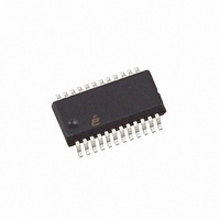
ISL6442IA Intersil, ISL6442IA Datasheet - Page 13

ISL6442IA
Manufacturer Part Number
ISL6442IA
Description
IC PWM BUCK VM 24QSOP
Manufacturer
Intersil
Datasheet
1.ISL6442IAZ-TK.pdf
(16 pages)
Specifications of ISL6442IA
Pwm Type
Voltage Mode
Number Of Outputs
3
Frequency - Max
2.85MHz
Duty Cycle
100%
Voltage - Supply
4.5 V ~ 24 V
Buck
Yes
Boost
No
Flyback
No
Inverting
No
Doubler
No
Divider
No
Cuk
No
Isolated
No
Operating Temperature
-40°C ~ 85°C
Package / Case
24-QSOP
Frequency-max
2.85MHz
Lead Free Status / RoHS Status
Contains lead / RoHS non-compliant
Available stocks
Company
Part Number
Manufacturer
Quantity
Price
Company:
Part Number:
ISL6442IAZ
Manufacturer:
Intersil
Quantity:
97
Company:
Part Number:
ISL6442IAZ
Manufacturer:
ST
Quantity:
6 267
Part Number:
ISL6442IAZ
Manufacturer:
INTERSIL
Quantity:
20 000
Part Number:
ISL6442IAZ-T
Manufacturer:
INTERSIL
Quantity:
20 000
Company:
Part Number:
ISL6442IAZ-TK
Manufacturer:
Intersil
Quantity:
6 000
The modulator transfer function is the small-signal transfer
function of V
gain, given by d
filter, with a double pole break frequency at F
F
channel inductance and its DCR, while C and E represent the
total output capacitance and its equivalent series resistance.
The compensation network consists of the error amplifier
(internal to the ISL6442) and the external R1-R3, C1-C3
components. The goal of the compensation network is to
provide a closed loop transfer function with high 0dB crossing
frequency (F
margin (better than 45°). Phase margin is the difference
between the closed loop phase at F
equations that follow relate the compensation network’s poles,
zeros and gain to the components (R1, R2, R3, C1, C2, and
C3) in Figure 14. Use the following guidelines for locating the
poles and zeros of the compensation network:
F
F
1. Select a value for R1 (1kΩ to 5kΩ, typically). Calculate
CE
FIGURE 14. VOLTAGE-MODE BUCK CONVERTER
LC
CE
value for R2 for desired converter bandwidth (F
setting the output voltage via an offset resistor connected
=
. For the purpose of this analysis, L and D represent the
=
CIRCUIT
---------------------------
2π
----------------------- -
2π C E
PWM
⋅
⋅
1
1
L C
COMP
OUT
0
⋅
⋅
; typically 0.1 to 0.3 of F
COMPENSATION DESIGN
MAX
/V
HALF-BRIDGE
OSCILLATOR
COMP
V
OSC
V
E/A
DRIVE
IN
R2
/V
ISL6442
. This function is dominated by a DC
C2
OSC
+
-
VREF
C1
13
, and shaped by the output
FB
UGATE
LGATE
PHASE
EXTERNAL CIRCUIT
0dB
SW
and 180°. The
R3
Ro
) and adequate phase
V
IN
R1
LC
C3
L
and a zero at
V
0
D
OUT
(EQ. 11)
(EQ. 10)
). If
C
E
ISL6442
It is recommended a mathematical model is used to plot the
loop response. Check the loop gain against the error
amplifier’s open-loop gain. Verify phase margin results and
adjust as necessary. The following equations describe the
frequency response of the modulator (G
compensation (G
G
where:
s f ( )
G
G
2. Calculate C1 such that F
3. Calculate C2 such that F
4. Calculate R3 such that F
MOD
FB
CL
to the FB pin, Ro in Figure 14, the design procedure can
be followed as presented in Equation 12.
at 0.1 to 0.75 of F
desired number). The higher the quality factor of the output
filter and/or the higher the ratio F
frequency (to maximize phase boost at F
such that F
times F
Change the numerical factor to reflect desired placement
of this pole. Placement of F
reduce the gain of the compensation network at high
frequency, in turn reducing the HF ripple component at
the COMP pin and minimizing resultant duty cycle jitter.
R2
C1
C2
R3
f ( )
=
f ( )
f ( )
2π f j
=
=
=
=
=
=
⋅
=
⋅ ⋅
----------------------------------------------------- - ⋅
s f ( ) R1
---------------------------------------------------------------------------------------------------------------------------- -
(
---------------------------------------------------------
2π R2 C1 F
--------------------- -
-------------------------------------------- -
d
----------------------------------------------- -
2π R2 0.5 F
F
----------- - 1
F
1
G
V
MAX
SW
SW
1
LC
d
----------------------------- -
+
MOD
OSC
R1
⋅
⋅
MAX
+
⋅
s f ( ) R3 C3
V
P2
). F
s f ( ) R2 C1
–
OSC
⋅
f ( ) G
⋅
V
⋅
⋅
FB
⋅
1
is placed below F
⋅
⋅
R1 F
SW
IN
C1
V
⋅
(
⋅
C1
) and closed-loop response (G
IN
1
⋅
LC
⋅
⋅
⋅
+
F
⋅
represents the switching frequency.
FB
⋅
⋅
+
LC
s f ( )
----------------------------------------------------------------------------------------
1
0
CE
LC
(to adjust, change the 0.5 factor to
C2
f ( )
+
)
s f ( )
–
⋅
Z1
⋅
)
P1
Z2
(
⎛
⎝
1
R1
1
C3
is placed at a fraction of the F
is placed at F
is placed at F
⋅
+
P2
(
1
+
s f ( ) R2
E
=
+
R3
+
SW
lower in frequency helps
CE
-------------------------------------------------
2π R3 0.7 F
s f ( ) E C
D
⋅
) C3
) C
/F
⋅
⋅
(typically, 0.5 to 1.0
⋅
⋅
LC
MOD
⋅
⎛
⎝
+
⋅
--------------------- -
C1
, the lower the F
⋅
C1 C2
1
CE
LC
LC
s
2
), feedback
f ( ) L C
+
. Calculate C3
).
⋅
.
⋅
C2
⋅
October 31, 2008
SW
(EQ. 12)
(EQ. 13)
(EQ. 14)
(EQ. 15)
⎞
⎠
CL
⋅
⎞
⎠
(EQ. 16)
(EQ. 17)
(EQ. 18)
):
FN9204.2
LC
Z1
,


