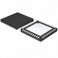
ISL8103IRZ Intersil, ISL8103IRZ Datasheet - Page 22

ISL8103IRZ
Manufacturer Part Number
ISL8103IRZ
Description
IC CTRLR PWM BUCK 3PHASE 40-QFN
Manufacturer
Intersil
Datasheet
1.ISL8103IRZ-T.pdf
(28 pages)
Specifications of ISL8103IRZ
Pwm Type
Voltage Mode
Number Of Outputs
1
Frequency - Max
1.5MHz
Duty Cycle
66.6%
Voltage - Supply
4.75 V ~ 12.6 V
Buck
Yes
Boost
No
Flyback
No
Inverting
No
Doubler
No
Divider
No
Cuk
No
Isolated
No
Operating Temperature
-40°C ~ 85°C
Package / Case
40-VFQFN, 40-VFQFPN
Frequency-max
1.5MHz
Lead Free Status / RoHS Status
Lead free / RoHS Compliant
Compensating the Converter operating without
Load-Line Regulation
The ISL8103 multiphase converter operating without load
line regulation behaves in a similar manner to a
voltage-mode controller. This section highlights the design
consideration for a voltage-mode controller requiring external
compensation. To address a broad range of applications, a
type-3 feedback network is recommended (see Figure 20).
Figure 21 highlights the voltage-mode control loop for a
synchronous-rectified buck converter, applicable, with a
small number of adjustments, to the mulitphase ISL8103
circuit. The output voltage (V
voltage, VREF, level. The error amplifier output (COMP pin
voltage) is compared with the oscillator (OSC) modified
saw-tooth wave to provide a pulse-width modulated wave with
an amplitude of V
smoothed by the output filter (L and C). The output filter
capacitor bank’s equivalent series resistance is represented by
the series resistor E.
The modulator transfer function is the small-signal transfer
function of V
gain, given by d
filter, with a double pole break frequency at F
F
the individual channel inductance and its DCR divided by 3
(equivalent parallel value of the three output inductors), while
C and ESR represents the total output capacitance and its
equivalent series resistance.
The compensation network consists of the error amplifier
(internal to the ISL8103) and the external R
components. The goal of the compensation network is to
provide a closed loop transfer function with high 0dB crossing
frequency (F
margin (better than 45°). Phase margin is the difference
between the closed loop phase at F
equations that follow relate the compensation network’s poles,
zeros and gain to the components (R
F
CE
LC
FIGURE 20. COMPENSATION CONFIGURATION FOR
=
. For the purpose of this analysis, L and DCR represent
---------------------------
2π
C
R
⋅
3
3
1
L C
OUT
0
⋅
; typically 0.1 to 0.3 of F
NON-LOAD-LINE REGULATED ISL8103 CIRCUIT
MAX
/V
IN
COMP
at the PHASE node. The PWM wave is
V
R
IN
R
1
2
/V
. This function is dominated by a DC
F
OSC
C
CE
2
OUT
C
=
22
1
, and shaped by the output
-------------------------------- -
2π C ESR
) is regulated to the reference
⋅
0dB
COMP
1
SW
VDIFF
1
⋅
, R
FB
and +180°. The
) and adequate phase
2
, R
1
-R
3
LC
, C
3
, C
ISL8103
and a zero at
1
1
, C
-C
2
3
(EQ. 29)
, and
ISL8103
C
locating the poles and zeros of the compensation network:
1. Select a value for R
2. Calculate C
FIGURE 21. VOLTAGE-MODE BUCK CONVERTER
3
) in Figure 20 and 21. Use the following guidelines for
value for R
If setting the output voltage to be equal to the reference
set voltage as shown in Figure 21, the design procedure
can be followed as presented. However, when setting the
output voltage via a resistor divider placed at the input of
the differential amplifier (as shown in Figure 6), in order
to compensate for the attenuation introduced by the
resistor divider, the obtained R
multiplied by a factor of (R
the calculations remain unchanged, as long as the
compensated R
at 0.1 to 0.75 of F
desired number). The higher the quality factor of the output
filter and/or the higher the ratio F
frequency (to maximize phase boost at F
R
C
CIRCUIT
2
1
PWM
=
=
-------------------------------------------- -
d
---------------------------------------------- -
2π R
V
COMP
MAX
OSC
⋅
COMPENSATION DESIGN
2
1
2
HALF-BRIDGE
⋅
OSCILLATOR
V
such that F
⋅
for desired converter bandwidth (F
⋅
1
V
0.5 F
R
IN
OSC
E/A
DRIVE
1
2
⋅
⋅
LC
⋅
R
F
value is used.
F
ISL8103
2
LC
0
LC
1
(to adjust, change the 0.5 factor to
C
+
-
+
(1kΩ to 5kΩ, typically). Calculate
VREF
2
-
Z1
C
1
is placed at a fraction of the F
P
+R
FB
PHASE
UGATE
LGATE
VDIFF
RGND
VSEN
EXTERNAL CIRCUIT
2
S
CE
)/R
value needs be
R
/F
3
V
P
LC
IN
. The remainder of
R
1
, the lower the F
LC
C
L
3
).
DCR
V
ESR
OUT
0
July 21, 2008
C
).
(EQ. 30)
(EQ. 31)
FN9246.1
LC
Z1
,


