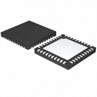
ISL8103IRZ Intersil, ISL8103IRZ Datasheet - Page 25

ISL8103IRZ
Manufacturer Part Number
ISL8103IRZ
Description
IC CTRLR PWM BUCK 3PHASE 40-QFN
Manufacturer
Intersil
Datasheet
1.ISL8103IRZ-T.pdf
(28 pages)
Specifications of ISL8103IRZ
Pwm Type
Voltage Mode
Number Of Outputs
1
Frequency - Max
1.5MHz
Duty Cycle
66.6%
Voltage - Supply
4.75 V ~ 12.6 V
Buck
Yes
Boost
No
Flyback
No
Inverting
No
Doubler
No
Divider
No
Cuk
No
Isolated
No
Operating Temperature
-40°C ~ 85°C
Package / Case
40-VFQFN, 40-VFQFPN
Frequency-max
1.5MHz
Lead Free Status / RoHS Status
Lead free / RoHS Compliant
For a three-phase design, use Figure 24 to determine the
input-capacitor RMS current requirement set by the duty
cycle, maximum sustained output current (I
of the peak-to-peak inductor current (I
bulk capacitor with a ripple current rating which will minimize
the total number of input capacitors required to support the
RMS current calculated. The voltage rating of the capacitors
should also be at least 1.25 times greater than the maximum
input voltage. Figures 25 and 26 provide the same input
RMS current information for two-phase and single-phase
designs respectively. Use the same approach for selecting
the bulk capacitor type and number.
FIGURE 24. NORMALIZED INPUT-CAPACITOR RMS
FIGURE 25. NORMALIZED INPUT-CAPACITOR RMS
0.3
0.2
0.1
0.3
0.2
0.1
0
0
0
0
I
I
I
I
I
L,P-P
L,P-P
L,P-P
L,P-P
L,P-P
CURRENT FOR 3-PHASE CONVERTER
CURRENT FOR 2-PHASE CONVERTER
= 0
= 0.5 I
= 0.75 I
= 0
= 0.25 I
0.2
0.2
O
O
O
DUTY CYCLE (V
DUTY CYCLE (V
0.4
0.4
25
I
I
L,P-P
L,P-P
0.6
0.6
IN/
IN/
= 0.5 I
= 0.75 I
L,P-P
V
V
O
O
)
)
) to I
O
O
O
), and the ratio
0.8
0.8
O
. Select a
1.0
1.0
ISL8103
Low ESL, high-frequency ceramic capacitors are needed in
addition to the input bulk capacitors to suppress leading and
falling edge voltage spikes. The spikes result from the high
current slew rate produced by the upper MOSFET turn on
and off. Place them as close as possible to each upper
MOSFET drain to minimize board parasitics and maximize
suppression.
Layout Considerations
MOSFETs switch very fast and efficiently. The speed with
which the current transitions from one device to another
causes voltage spikes across the interconnecting
impedances and parasitic circuit elements. These voltage
spikes can degrade efficiency, radiate noise into the circuit
and lead to device overvoltage stress. Careful component
layout and printed circuit design minimizes the voltage
spikes in the converter. Consider, as an example, the turnoff
transition of the upper PWM MOSFET. Prior to turnoff, the
upper MOSFET was carrying channel current. During the
turnoff, current stops flowing in the upper MOSFET and is
picked up by the lower MOSFET. Any inductance in the
switched current path generates a large voltage spike during
the switching interval. Careful component selection, tight
layout of the critical components, and short, wide circuit
traces minimize the magnitude of voltage spikes.
There are two sets of critical components in a DC/DC
converter using a ISL8103 controller. The power
components are the most critical because they switch large
amounts of energy. Next are small signal components that
connect to sensitive nodes or supply critical bypassing
current and signal coupling.
It is important to have a symmetrical layout, preferably with
the controller equidistantly located from the three power
trains it controls. Equally important are the gate drive lines
(UGATE, LGATE, PHASE): since they drive the power train
FIGURE 26. NORMALIZED INPUT-CAPACITOR RMS
0.6
0.4
0.2
0
0
I
I
I
CURRENT FOR SINGLE-PHASE CONVERTER
L,P-P
L,P-P
L,P-P
0.2
= 0
= 0.5 I
= 0.75 I
DUTY CYCLE (V
O
0.4
O
0.6
IN
/V
O
)
0.8
July 21, 2008
FN9246.1
1.0


