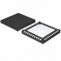
ISL6264CRZ Intersil, ISL6264CRZ Datasheet - Page 19

ISL6264CRZ
Manufacturer Part Number
ISL6264CRZ
Description
IC CORE CTRLR TWO-PHASE 40-QFN
Manufacturer
Intersil
Datasheet
1.ISL6264CRZ.pdf
(23 pages)
Specifications of ISL6264CRZ
Applications
Controller, AMD Mobile Turion™
Voltage - Input
5 ~ 24 V
Number Of Outputs
1
Voltage - Output
0.38 ~ 1.55 V
Operating Temperature
-10°C ~ 100°C
Mounting Type
Surface Mount
Package / Case
40-VFQFN, 40-VFQFPN
Lead Free Status / RoHS Status
Lead free / RoHS Compliant
Available stocks
Company
Part Number
Manufacturer
Quantity
Price
Part Number:
ISL6264CRZ
Manufacturer:
INTERSIL
Quantity:
20 000
Company:
Part Number:
ISL6264CRZ-T
Manufacturer:
INTERSIL
Quantity:
4 093
Part Number:
ISL6264CRZ-T
Manufacturer:
INTERSIL
Quantity:
20 000
Setting the Switching Frequency - FSET
The R3 modulator scheme is not a fixed frequency PWM
architecture. The switching frequency can increase during
the application of a load to improve transient performance.
It also varies slightly due changes in input and output voltage
and output current, but this variation is normally less than
10% in continuous conduction mode.
Refer to Figure 2. The resistor connected between the VW
and COMP pins of the ISL6264 adjusts the switching
window, and therefore adjusts the switching frequency. The
RFSET resistor that sets up the switching frequency of the
controller operating in CCM can be determined using the
following relationship, where RFSET is in kΩ and the
switching period is in µs. 6.81kΩ sets about 300kHz
switching frequency (see Equation 5).
In discontinuous conduction mode (DCM), the ISL6264 runs
into period stretching mode. The switching frequency is
dependent on the load current level. In general, the lighter
load, the slower switching frequency. Therefore, the
switching loss is much reduced for the light load operation,
which is important for conserving the battery power in the
portable application.
Static Mode of Operation - Static Droop Using DCR
Sensing
As previously mentioned, the ISL6264 has an internal
differential amplifier which provides very accurate voltage
regulation at the die of the processor. The load line
regulation is also accurate for both two-phase and
single-phase operation. The process of selecting the
components for the appropriate load line droop is explained
here.
For DCR sensing, the process of compensation for DCR
resistance variation to achieve the desired load line droop
has several steps and is somewhat iterative.
R
FSET
OC
(
kΩ
INTERNAL TO
FIGURE 32. SIMPLIFIED SCHEMATIC FOR DROOP AND DIE SENSING WITH INDUCTOR DCR CURRENT SENSING
VD IFF
)
∼
ISL6264
(
period μs
S
-
+
+
+
(
10µA
) 0.4
1
1
RTN
–
+
+
-
-
19
) 2.33
⋅
DROOP
VSEN
+
-
DR OOP
OC SE T
VSUM
DFB
VO'
(EQ. 5)
ISL6264
The two-phase solution using DCR sensing is shown in
Figure 31. There are two resistors connecting to the
terminals of inductor of each phase. These are labeled RS
and R
drop across each inductor. Each inductor will have a certain
level of DC current flowing through it, and this current when
multiplied by the DCR of the inductor creates a small DC
voltage drop across the inductor terminal. When this voltage
is summed with the other channels DC voltages, the total DC
load current can be derived.
R
outputs of all channels together and thus create a summed
average of the local CORE voltage output. R
through an understanding of both the DC and transient load
currents. This value will be covered in the next section.
However, it is important to keep in mind that the output of
each of these R
VSUM voltage node. With both the outputs of R
together, the simplified model for the droop circuit can be
derived. This is presented in Figure 32.
Essentially one resistor can replace the R
phase and one R
each phase. The total DCR drop due to load current can be
replaced by a DC source, the value of which is given by:
For the convenience of analysis, the NTC network
comprised of R
labelled as a single resistor R
The first step in droop load line compensation is to adjust R
R
even at light loads between the VSUM and VO' nodes. As a
rule of thumb we start with the voltage drop across the R
network, VN, to be 0.5-0.8 times VDCR_EQU. This ratio
provides for a fairly reasonable amount of light load signal
from which to arrive at droop.
V
VSUM
O
OEQV
VN
DCR_EQU
VO '
+
-
is typically 1Ω to 10Ω. This resistor is used to tie the
O
. These resistors are used to obtain the DC voltage
and R
=
SEQV
I
------------------------------- -
OUT
ntc
S
S
, R
resistors are tied together to create the
2
⋅
resistor can replace the R
such that sufficient droop voltage exists
DCR
series
Vdcr
RS
and R
EQV
EQV
n
=
in Figure 32.
par
=
RS
------- -
2
, given in Figure 31, is
I
OUT
×
DCR
-------------
O
2
resistors of each
S
S
is determined
O
resistors of
and R
May 28, 2009
FN6359.3
(EQ. 6)
S
tied
n
n
,


