ISL6264CRZ Intersil, ISL6264CRZ Datasheet - Page 5
ISL6264CRZ
Manufacturer Part Number
ISL6264CRZ
Description
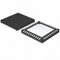
IC CORE CTRLR TWO-PHASE 40-QFN
Manufacturer
Intersil
Datasheet
1.ISL6264CRZ.pdf
(23 pages)
Specifications of ISL6264CRZ
Applications
Controller, AMD Mobile Turion™
Voltage - Input
5 ~ 24 V
Number Of Outputs
1
Voltage - Output
0.38 ~ 1.55 V
Operating Temperature
-10°C ~ 100°C
Mounting Type
Surface Mount
Package / Case
40-VFQFN, 40-VFQFPN
Lead Free Status / RoHS Status
Lead free / RoHS Compliant
Available stocks
Company
Part Number
Manufacturer
Quantity
Price

Part Number:
ISL6264CRZ
Manufacturer:
INTERSIL
Quantity:
20 000
Company:
Part Number:
ISL6264CRZ-T
Manufacturer:
INTERSIL
Quantity:
4 093
Part Number:
ISL6264CRZ-T
Manufacturer:
INTERSIL
Quantity:
20 000


Functional Pin Description
OCSET
SET
Logic low enables the audio filter which only allows above
20kHz operation. Logic high disables the audio filter.
RBIAS
147kΩ resistor to GND sets internal current reference,
~10µA, for the overcurrent protection setting.
OFS
A resistor from this pin to GND programs a DC current
source for generating a positive offset voltage across the
resistor between FB and VDIFF pins. The OFS pin voltage is
1.2V.
SOFT
A capacitor from this pin to GND pin sets the maximum slew
rate of the output voltage. The SOFT pin is the non-inverting
input of the error amplifier. A 210µA internal current source is
generated to charge or discharge the SOFT pin capacitor to
determine the slew-rate of VID. During the start-up process,
the current source is reduced to 43µA.
OCSET
Overcurrent protection set input. A resistor from this pin to
VO sets DROOP voltage limit for OC trip. A 10µA current
source is connected internally to this pin.
VW
A resistor from this pin to COMP programs the switching
frequency (for example, 6.81k ~ 300kHz).
COMP
This pin is the output of the error amplifier.
RBIAS
COMP
VDIFF
SOFT
VSEN
OFS
SET
VW
FB
10
1
2
3
4
5
6
7
8
9
40
11 12 13 14 15 16 17 18 19 20
39 38 37 36 35 34 33 32 31
(BOTTOM)
GND PAD
5
30
29
28
27
26
25
24
23
22
21
UGATE1
PHASE1
PGND1
LGATE1
PVCC
LGATE2
PGND2
PHASE2
UGATE2
BOOT2
ISL6264
FB
This pin is the inverting input of the error amplifier.
VDIFF
This pin is the output of the differential amplifier.
VSEN
Remote core voltage sense input.
RTN
Remote core voltage sense return.
DROOP
Output of the droop amplifier. The voltage level at this pin is
the sum of Vo and the programmed droop voltage by the
external resistors.
DFB
This pin is the inverting input of the droop amplifier.
VO
An input to IC reporting the local output voltage.
VSUM
This pin is connected to the summation junction of channel
current sensing.
VIN
It is used for input voltage feed forward to improve input line
transient performance.
GND
Signal ground. Connect to local controller ground.
VCC
5V bias power supply for the ISL6264 controller.
ISEN2
Individual current sharing sensing for channel 2.
ISEN1
Individual current sharing sensing for channel 1.
BOOT2
This pin is the upper gate driver supply voltage for phase 2.
An internal boot strap diode is connected to the PVCC pin.
UGATE2
Upper MOSFET gate signal for phase 2.
PHASE2
The phase node of phase 2. This pin should connect to the
source of upper MOSFET. It is the return path for the upper
MOSFET drive.
PGND2
The return path of the lower gate driver for phase 2.
LGATE2
Lower-side MOSFET gate signal for phase 2.
May 28, 2009
FN6359.3
Related parts for ISL6264CRZ
Image
Part Number
Description
Manufacturer
Datasheet
Request
R

Part Number:
Description:
Intersil Corporation [CMOS Serial Controller Interface]
Manufacturer:
Intersil Corporation
Datasheet:
Part Number:
Description:
Manufacturer:
Intersil Corporation
Datasheet:
Part Number:
Description:
357-036-542-201 CARDEDGE 36POS DL .156 BLK LOPRO
Manufacturer:
Intersil Corporation
Datasheet:
Part Number:
Description:
1024-Word x 4-Bit LSI Static RAM
Manufacturer:
Intersil Corporation
Datasheet:
Part Number:
Description:
General Purpose NPN Transistor Arrays FN341.4
Manufacturer:
Intersil Corporation
Datasheet:
Part Number:
Description:
CMOS 16-Bit Microprocessor
Manufacturer:
Intersil Corporation
Datasheet:
Part Number:
Description:
Manufacturer:
Intersil Corporation
Datasheet:
Part Number:
Description:
Manufacturer:
Intersil Corporation
Datasheet:
Part Number:
Description:
Manufacturer:
Intersil Corporation
Datasheet:
Part Number:
Description:
Manufacturer:
Intersil Corporation
Datasheet:
Part Number:
Description:
CMOS 6-Bit Latch and Decoder Memory Interfaces
Manufacturer:
Intersil Corporation
Datasheet:
Part Number:
Description:
CA3046General Purpose NPN Transistor Arrays
Manufacturer:
Intersil Corporation
Datasheet:
Part Number:
Description:
Manufacturer:
Intersil Corporation
Datasheet:
Part Number:
Description:
TR909 DLC/FLC SLIC with Low Power Standby
Manufacturer:
Intersil Corporation
Datasheet: