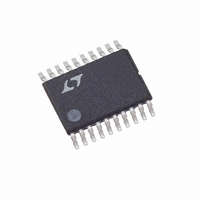
LTC3417AIFE-1#PBF Linear Technology, LTC3417AIFE-1#PBF Datasheet - Page 13

LTC3417AIFE-1#PBF
Manufacturer Part Number
LTC3417AIFE-1#PBF
Description
IC BUCK SYNC ADJ 1A/1.5A 20TSSOP
Manufacturer
Linear Technology
Type
Step-Down (Buck)r
Datasheet
1.LTC3417AEDHC-1PBF.pdf
(20 pages)
Specifications of LTC3417AIFE-1#PBF
Internal Switch(s)
Yes
Synchronous Rectifier
Yes
Number Of Outputs
2
Voltage - Output
0.8 ~ 5 V
Current - Output
1A, 1.5A
Frequency - Switching
1.5MHz, 0.6MHz ~ 4MHz
Voltage - Input
2.25 ~ 5.5 V
Operating Temperature
-40°C ~ 125°C
Mounting Type
Surface Mount
Package / Case
20-TSSOP Exposed Pad, 20-eTSSOP, 20-HTSSOP
Lead Free Status / RoHS Status
Lead free / RoHS Compliant
Power - Output
-
APPLICATIONS INFORMATION
Soft-Start
Soft-start reduces surge currents from V
ally increasing the peak inductor current. Power supply
sequencing can also be accomplished by controlling the
I
for each regulator output, which steps up a clamp on
I
and 3. As the voltage on I
range, the internal peak current limit is also ramped at a
proportional linear rate.
Mode Selection
The SYNC/MODE pin is a multipurpose pin which provides
mode selection and frequency synchronization. Connect-
ing this pin to V
regulators, which provides the best low current effi ciency
at the cost of a higher output voltage ripple. When SYNC/
MODE is connected to ground, pulse skipping operation
is selected for both regulators, which provides the low-
est output voltage and current ripple at the cost of low
current effi ciency. Applying a voltage that is more than
1V from either supply results in forced continuous mode
for both regulators, which creates a fi xed output ripple
and allows the sinking of some current (about 1/2ΔI
Since the switching noise is constant in this mode, it is
also the easiest to fi lter out. In many cases, the output
voltage can be simply connected to the SYNC/MODE pin,
selecting the forced continuous mode except at start-up.
TH
TH
pin. The LTC3417A-1 has an internal digital soft-start
over 1024 clock cycles, as can be seen in Figures 2
2V/DIV
1V/DIV
1A/DIV
V
V
RUN
OUT
I
L
V
V
R
Figure 2. Digital Soft-Start OUT1
IN
OUT
L
= 0.9Ω
IN
= 3.6V
= 1.8V
enables Burst Mode operation for both
200μs/DIV
TH
ramps through its operating
3417A-1 F02
IN
by gradu-
L
).
The LTC3417A-1 can be synchronized to an external clock
signal by the SYNC/MODE pin. The internal oscillator fre-
quency should be set to 20% lower than the external clock
frequency to ensure adequate slope compensation, since
slope compensation is derived from the internal oscillator.
During synchronization, the mode is set to pulse skipping
and the top switch turn-on is synchronized to the rising
edge of the external clock.
When using an external clock, with the PHASE pin low, the
switching of the two channels occur at the edges of the
external clock. A 50% duty cycle will therefore produce
180° out-of-phase operation.
Checking Transient Response
The I
to be optimized for a wide range of loads and output
capacitors. The availability of the I
optimization of the control loop behavior, but also pro-
vides a DC coupled and AC fi lited closed-loop response
test point. The DC step, rise time, and settling at this test
point truly refl ects the closed-loop response. Assuming a
predominantly second order system, phase margin and/or
or damping factor can be estimated using the percentage
of overshoot seen at this pin. The bandwidth can also be
estimated using the percentage of overshoot seen at this
pin or by examining the rise time at this pin.
TH
0.5A/DIV
2V/DIV
1V/DIV
pin compensation allows the transient response
V
V
RUN
OUT
I
L
V
V
R
IN
OUT
L
Figure 3. Digital Soft-Start OUT2
= 2Ω
= 3.6V
= 2.5V
200μs/DIV
LTC3417A-1
TH
pin not only allows
3417A-1 F03
13
3417a1fa


