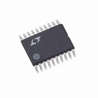
LTC3417AIFE-1#PBF Linear Technology, LTC3417AIFE-1#PBF Datasheet - Page 6

LTC3417AIFE-1#PBF
Manufacturer Part Number
LTC3417AIFE-1#PBF
Description
IC BUCK SYNC ADJ 1A/1.5A 20TSSOP
Manufacturer
Linear Technology
Type
Step-Down (Buck)r
Datasheet
1.LTC3417AEDHC-1PBF.pdf
(20 pages)
Specifications of LTC3417AIFE-1#PBF
Internal Switch(s)
Yes
Synchronous Rectifier
Yes
Number Of Outputs
2
Voltage - Output
0.8 ~ 5 V
Current - Output
1A, 1.5A
Frequency - Switching
1.5MHz, 0.6MHz ~ 4MHz
Voltage - Input
2.25 ~ 5.5 V
Operating Temperature
-40°C ~ 125°C
Mounting Type
Surface Mount
Package / Case
20-TSSOP Exposed Pad, 20-eTSSOP, 20-HTSSOP
Lead Free Status / RoHS Status
Lead free / RoHS Compliant
Power - Output
-
LTC3417A-1
TYPICAL PERFORMANCE CHARACTERISTICS
RUN1 (Pin 1/Pin 2): Enable for 1.5A Regulator. When
at Logic 1, 1.5A regulator is running. When at 0V, 1.5A
regulator is off. When both RUN1 and RUN2 are at 0V, the
part is in shutdown.
V
1.5A Regulator.
I
for 1.5A Regulator. The current comparator threshold
increases with this control voltage. Nominal voltage range
for this pin is 0V to 1.5V.
V
external resistive divider across the 1.5A regulator output.
Nominal voltage for this pin is 0.8V.
V
external resistive divider across the 1A regulator output.
Nominal voltage for this pin is 0.8V.
I
1A regulator. The current comparator threshold increases
with this control voltage. Nominal voltage range for this
pin is 0V to 1.5V.
RUN2 (Pin 7/Pin 8): Enable for 1A Regulator. When at
Logic 1, 1A regulator is running. When at 0V, 1A regula-
tor is off. When both RUN1 and RUN2 are at 0V, the part
is in shutdown.
V
Regulator and Supply for Analog Circuitry.
6
PIN FUNCTIONS
TH1
TH2
IN1
FB1
FB2
IN2
0.14
0.20
0.19
0.18
0.17
0.16
0.15
(Pin 6/Pin 7): Error Amplifi er Compensation Point for
(Pin 8/Pin 9): Supply Pin for P-Channel Switch of 1A
(Pin 3/Pin 4): Error Amplifi er Compensation Point
(Pin 2/Pin 3): Supply Pin for P-Channel Switch of
(Pin 4/Pin 5): Receives the feedback voltage from
(Pin 5/Pin 6): Receives the feedback voltage from
R
2
DS(ON)
N-CHANNEL SWITCH
2.5
P-CHANNEL SWITCH
vs V
3
IN
3.5
OUT2
V
IN
(V)
4
(DFN/TSSOP)
4.5
T
A
= 27°C
5
3417A-1 G16
5.5
–10
–2
–4
–6
–8
4
2
0
6
2
Frequency vs V
FREQ = 143k TO GROUND
2.5
FREQ = V
3
3.5
V
IN
IN
SYNC/MODE (Pin 9/Pin 12): Combination Mode Selection
and Oscillator Synchronization Pin. This pin controls the op-
eration of the device. When the voltage on the SYNC/MODE
pin is >(V
When the voltage on the SYNC/MODE pin is <0.5V, pulse
skipping mode is selected. When the SYNC/MODE pin is
held at V
oscillation frequency can be synchronized to an external
oscillator applied to this pin. When synchronized to an
external clock, pulse skip mode is selected.
SW2 (Pin 10/Pin 13): Switch Node Connection to the
Inductor for the 1A Regulator. This pin swings from V
to PGND2.
POR (Pin 11/Pin 14): The Power-On-Reset Pin. This
open drain-logic output is pulled to GND when the output
voltage of either regulator falls 8% below regulation and
goes high approximately 150ms after both regulators are
above –6% of regulation. If either RUN1 or RUN2 is low
(the respective regulator is in sleep mode and therefore
the output voltage is low), then POR refl ects the regulation
of the running regulator.
FREQ (Pin 12/Pin 15): Frequency Set Pin. When FREQ is
at V
is connected from this pin to ground, the internal oscillator
frequency can be varied from 0.6MHz to 4MHz.
GNDA (Pin 13/Pin 16): Analog Ground Pin for Internal
Analog Circuitry.
IN
(V)
4
IN
, internal oscillator runs at 1.5MHz. When a resistor
4.5
IN
IN
/2, forced continuous mode is selected. The
3417A-1 G17
5
– 0.5V), Burst Mode operation is selected.
5.5
–15
–10
15
10
–5
0
5
–50
Frequency vs Temperature
–25
0
TEMPERATURE (°C)
25
FREQ = V
FREQ = 143k TO GROUND
50
IN
75
100
3417A-1 G18
3417a1fa
IN2
125


