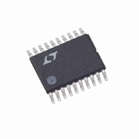
LTC3417AIFE-1#PBF Linear Technology, LTC3417AIFE-1#PBF Datasheet - Page 9

LTC3417AIFE-1#PBF
Manufacturer Part Number
LTC3417AIFE-1#PBF
Description
IC BUCK SYNC ADJ 1A/1.5A 20TSSOP
Manufacturer
Linear Technology
Type
Step-Down (Buck)r
Datasheet
1.LTC3417AEDHC-1PBF.pdf
(20 pages)
Specifications of LTC3417AIFE-1#PBF
Internal Switch(s)
Yes
Synchronous Rectifier
Yes
Number Of Outputs
2
Voltage - Output
0.8 ~ 5 V
Current - Output
1A, 1.5A
Frequency - Switching
1.5MHz, 0.6MHz ~ 4MHz
Voltage - Input
2.25 ~ 5.5 V
Operating Temperature
-40°C ~ 125°C
Mounting Type
Surface Mount
Package / Case
20-TSSOP Exposed Pad, 20-eTSSOP, 20-HTSSOP
Lead Free Status / RoHS Status
Lead free / RoHS Compliant
Power - Output
-
OPERATION
Dropout Operation
When the input supply voltage decreases toward the output
voltage, the duty cycle increases to 100%. In this dropout
condition, the PMOS switch is turned on continuously with
the output voltage being equal to the input voltage minus
the voltage drops across the internal P-channel MOSFET
and inductor.
APPLICATIONS INFORMATION
A general LTC3417A-1 application circuit is shown in
Figure 4. External component selection is driven by the
load requirement, and begins with the selection of the
inductors L1 and L2. Once L1 and L2 are chosen, C
C
Operating Frequency
Selection of the operating frequency is a tradeoff between
effi ciency and component size. High frequency operation
allows the use of smaller inductor and capacitor values.
Operation at lower frequencies improves effi ciency by
reducing internal gate charge losses but requires larger
inductance values and/or capacitance to maintain low
output ripple voltage.
The operating frequency, f
mined by pulling the FREQ pin to V
tion or by connecting an external resistor from FREQ to
ground. The value of the resistor sets the ramp current
that is used to charge and discharge an internal timing
capacitor within the oscillator and can be calculated by
using the following equation:
for 0.6MHz ≤ f
select the value for R
The maximum operating frequency is also constrained
by the minimum on-time and duty cycle. This can be
calculated as:
OUT1
R
T
≈
and C
1.61• 10
OUT2
f
O
O
11
can be selected.
≤ 4MHz. Alternatively, use Figure 1 to
( )
Ω
T
.
– 16.586kΩ
O
, of the LTC3417A-1 is deter-
IN
for 1.5MHz opera-
IN
,
Low Supply Operation
The LTC3417A-1 incorporates an undervoltage lockout
circuit which shuts down the part when the input voltage
drops below about 2.07V to prevent unstable operation.
The minimum frequency is limited by leakage and noise
coupling due to the large resistance of R
Inductor Selection
Although the inductor does not infl uence the operating
frequency, the inductor value has a direct effect on ripple
current. The inductor ripple current, ΔI
higher inductance and increases with higher V
V
Accepting larger values of ΔI
tances, but results in higher output voltage ripple, greater
core losses and lower output current capability.
OUT
f
O(MAX)
.
I
L
=
V
f
160
140
120
100
O
80
60
40
20
OUT
0
• L
0
6.67
0.5 1.0
Figure 1. Frequency vs R
1–
V
V
IN(MAX)
V
OUT
V
1.5
FREQUENCY (MHz)
IN
OUT
2.0
L
2.5
allows the use of low induc-
(
MHz
3.0
LTC3417A-1
3.5
)
3417A-1 F01
T
4.0
L
, decreases with
T
.
4.5
3417a1fa
IN
9
or


