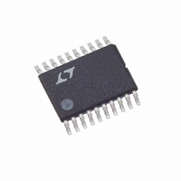
LTC3417AIFE-1#PBF Linear Technology, LTC3417AIFE-1#PBF Datasheet - Page 7

LTC3417AIFE-1#PBF
Manufacturer Part Number
LTC3417AIFE-1#PBF
Description
IC BUCK SYNC ADJ 1A/1.5A 20TSSOP
Manufacturer
Linear Technology
Type
Step-Down (Buck)r
Datasheet
1.LTC3417AEDHC-1PBF.pdf
(20 pages)
Specifications of LTC3417AIFE-1#PBF
Internal Switch(s)
Yes
Synchronous Rectifier
Yes
Number Of Outputs
2
Voltage - Output
0.8 ~ 5 V
Current - Output
1A, 1.5A
Frequency - Switching
1.5MHz, 0.6MHz ~ 4MHz
Voltage - Input
2.25 ~ 5.5 V
Operating Temperature
-40°C ~ 125°C
Mounting Type
Surface Mount
Package / Case
20-TSSOP Exposed Pad, 20-eTSSOP, 20-HTSSOP
Lead Free Status / RoHS Status
Lead free / RoHS Compliant
Power - Output
-
PIN FUNCTIONS
PHASE (Pin 14/Pin 17): Selects 1A regulator switching
phase with respect to 1.5A regulator switching. Set to
V
When PHASE is at 0V, the 1.5A regulator and the 1A
regulator are switching 180 degrees out-of-phase. Do
not fl oat this pin.
SW1 (Pin 15/Pin 18): Switch Node Connection to the
Inductor for the 1.5A Regulator. This pin swings from
V
FUNCTIONAL DIAGRAM
IN
IN1
, the 1.5A regulator and the 1A regulator are in phase.
to PGND1.
1.5A REGULATOR
1A REGULATOR
V FB1
RUN1
SYNC/MODE
V
RUN2
FB2
REFERENCE
VOLTAGE
0.752V
0.848V
0.848V
0.752V
+
–
+
–
+
–
–
+
–
+
–
+
V
IN2
V B
V
B
I TH1
I
TH2
–
+
+
–
PGND1 (Pin 16/Pin 19): Ground for SW1 N-Channel Driver.
PGND2, GNDD (Pins 1,10,11,20): TSSOP Package Only.
Ground for SW2 N-channel driver and digital ground for
circuit.
Exposed Pad (Pin 17/Pin 21): PGND2, GNDD. Ground for
SW2 N-channel driver and digital ground for circuit. The
Exposed Pad must be soldered to PCB ground.
LIMIT
LOGIC
LOGIC
LIMIT
I TH
I
TH
COMPENSATION
COMPENSATION
ANTI-SHOOT-
ANTI-SHOOT-
THROUGH
THROUGH
SLOPE
SLOPE
OSCILLATOR
+
+
+
+
+
+
–
–
–
–
–
–
DELAY
V IN1
V
IN2
PGND1
PGND2
PHASE
FREQ
SW1
SW2
POR
3417A-1 BD
LTC3417A-1
3417a1fa
7


