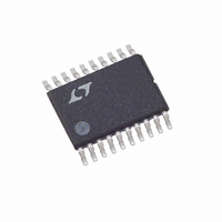
LTC3417AIFE-1#PBF Linear Technology, LTC3417AIFE-1#PBF Datasheet - Page 18

LTC3417AIFE-1#PBF
Manufacturer Part Number
LTC3417AIFE-1#PBF
Description
IC BUCK SYNC ADJ 1A/1.5A 20TSSOP
Manufacturer
Linear Technology
Type
Step-Down (Buck)r
Datasheet
1.LTC3417AEDHC-1PBF.pdf
(20 pages)
Specifications of LTC3417AIFE-1#PBF
Internal Switch(s)
Yes
Synchronous Rectifier
Yes
Number Of Outputs
2
Voltage - Output
0.8 ~ 5 V
Current - Output
1A, 1.5A
Frequency - Switching
1.5MHz, 0.6MHz ~ 4MHz
Voltage - Input
2.25 ~ 5.5 V
Operating Temperature
-40°C ~ 125°C
Mounting Type
Surface Mount
Package / Case
20-TSSOP Exposed Pad, 20-eTSSOP, 20-HTSSOP
Lead Free Status / RoHS Status
Lead free / RoHS Compliant
Power - Output
-
APPLICATIONS INFORMATION
LTC3417A-1
Board Layout Considerations
When laying out the printed circuit board, the following
checklist should be used to ensure proper operation of the
LTC3417A-1. These items are also illustrated graphically
in the layout diagram of Figure 5. Check the following in
your layout.
1. Does the capacitor C
2. Are the C
3. The resistor divider, R1 and R2, must be connected
18
(Pin 2), V
close as possible (DFN package)? It may be necessary
to split C
the AC current to the internal power MOSFETs and
their drivers.
(–) plate of C
(–) plate of C
and the (–) plate of C
between the (+) plate of C
minated near GNDA. The resistor divider, R3 and R4,
IN
OUT1
IN2
into two capacitors. This capacitor provides
OUT2
, L
OUT1
(Pin 8), and PGND2/GNDD (Pin 17) as
1
and C
returns current to the PGND2/GNDD
returns current to PGND1, and the
STAR TO
IN
GNDA
IN
OUT2
C
V
.
OUT2
OUT2
V
V
IN
IN
connect to the power V
OUT1
, L
10μF
C
2
IN
closely connected? The
C
and a ground line ter-
ITH2
C
0.1μF
C2
C
R
IN2
R3
R4
R8
L2
ITH2
Figure 5. Layout Guideline
V
PGND2/
EXPOSED PAD
GNDA
SW2
V
I
POR
RUN2
PHASE
TH2
IN2
FB2
IN1
LTC3417A-1
GNDD
SYNC/MODE
4. Keep sensitive components away from the SW pins.
5. A ground plane is preferred, but if not available, keep
6. Flood all unused areas on all layers with copper. Flooding
PGND1
RUN1
FREQ
must be connected between the (+) plate of C
a ground line terminated near GNDA. The feedback
signals V
components and traces, such as the SW lines, and its
trace should be minimized.
The input capacitor C
C
R4, R
SW traces and the inductors L1 and L2.
the signal and power grounds segregated with small
signal components returning to the GNDA pin at one
point which is then connected to the PGND2/GNDD
pin.
with copper will reduce the temperature rise of power
components. These copper areas should be connected
to one of the input supplies.
SW1
V
V
I
TH1
FB1
IN1
C1
, C
ITH1
C2
, C
FB1
R
ITH1
and R
L1
R1
R2
R7
C
0.1μF
ITH1
IN1
and V
C
C1
3417A-1 F05
C
and C
ITH1
ITH2
FB2
should be routed away from noise
should be routed away from the
ITH2
IN
STAR TO
GNDA
C
V
V
, the compensation capacitors
OUT1
OUT1
IN
and all resistors R1, R2, R3,
OUT2
3417a1fa
and


