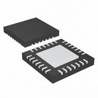
DS1865T+T&R Maxim Integrated Products, DS1865T+T&R Datasheet - Page 8

DS1865T+T&R
Manufacturer Part Number
DS1865T+T&R
Description
IC PON CONTROL TRI 28-TQFN
Manufacturer
Maxim Integrated Products
Datasheet
1.DS1865TTR.pdf
(66 pages)
Specifications of DS1865T+T&R
Applications
*
Mounting Type
Surface Mount
Package / Case
28-TQFN Exposed Pad
Lead Free Status / RoHS Status
Lead free / RoHS Compliant
PON Triplexer Control and
Monitoring Circuit
8
7, 10, 11,
26, 27,
12–15
5, 19
6, 18
PIN
25
16
17
20
21
22
23
24
28
—
_____________________________________________________________________
1
2
3
4
8
9
MON1–MON4
D1, D2, D3
M4DAC
NAME
DAC1
FETG
MOD
TX-D
GND
BIAS
BMD
LOSI
BEN
TX-F
N.C.
SDA
V
SCL
D0
EP
CC
Burst Enable Input. Triggers the sampling of the APC and quick-trip monitors.
Transmit Disable Input. Disables BIAS and MOD outputs.
Transmit Fault Output, Open Drain
Output to FET Gate. Signals an external n- or p-channel MOSFET to enable/disable the laser’s current.
Supply Voltage
Ground
No Connection
I
I
External Monitor Input 1–4. The voltage at these pins are digitized by the internal analog-to-digital
converter and can be read through the I
interrupt the processor based on the ADC result.
Digital-to-Analog Output DAC1 and M4DAC. Two 8-bit DAC outputs for generating analog voltages.
Typically used to control the video photodiode bias. M4DAC is controlled by the input voltage on MON4
and Table 06h LUT.
Bias Current Output. This current DAC generates the bias current reference for the MAX3643.
Modulation Output Voltage. This 8-bit voltage output has eight full-scale ranges from 1.25V to 0.3125V.
This pin is connected to the MAX3643’s VMSET input to control the modulation current.
Monitor Diode Input (Feedback Voltage, Transmit Power Monitor)
Loss-of-Signal Input. This input is accessible in the status register through the I
Digital I/O 0. This signal is either the open-drain output driver for LOSI, or can be controlled by the
OUT0 bit (D0OUT). The logic level of this pin is indicated by the D0IN and LOS status bits.
Digital I/O 1–3. These are bidirectional pins controlled by internally addressable bits. The outputs are
open-drain.
Exposed Pad. This contact should be connected to GND.
2
2
C Serial Data. Input/output for I
C Serial Clock. Input for I
2
C clock.
2
C data.
2
C interface. Alarm and warning values can be assigned to
FUNCTION
Pin Description
2
C interface.


