MCP1631RD-MCC1 Microchip Technology, MCP1631RD-MCC1 Datasheet - Page 187
MCP1631RD-MCC1
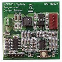
Manufacturer Part Number
MCP1631RD-MCC1
Description
REFERENCE DESIGN FOR MCP1631HV
Manufacturer
Microchip Technology
Type
Battery Managementr
Datasheets
1.MCP1631VHVT-330EST.pdf
(34 pages)
2.MCP1631HV-330EST.pdf
(54 pages)
3.MCP1631RD-MCC2.pdf
(20 pages)
4.MCP1631RD-MCC2.pdf
(328 pages)
5.MCP1631RD-MCC1.pdf
(28 pages)
Specifications of MCP1631RD-MCC1
Main Purpose
Power Management, Battery Charger
Embedded
Yes, MCU, 8-Bit
Utilized Ic / Part
MCP1631HV, PIC16F883
Primary Attributes
1 ~ 2 Cell- Li-Ion, 1 ~ 4 Cell- NiCd/NiMH
Secondary Attributes
Status LEDs
Supported Devices
MCP1631HV, PIC16F883 Device Type
Tool / Board Applications
Power Management-Battery Management
Development Tool Type
Reference Design
Input Voltage
5.5 V to 16 V
Product
Power Management Modules
Mcu Supported Families
MCP1631HV/PIC16F883 Family
Silicon Manufacturer
Microchip
Silicon Core Number
MCP1631HV
Kit Application Type
Reference Design
Application Sub Type
Battery Charger
Kit Contents
Board Only
Lead Free Status / RoHS Status
Lead free / RoHS Compliant
For Use With/related Products
MCP1631HV, PIC16F883
Lead Free Status / RoHS Status
Lead free / RoHS Compliant


13.3.3
The master can initiate the data transfer at any time
because it controls the SCK. The master determines
when the slave is to broadcast data by the software
protocol.
In Master mode, the data is transmitted/received as
soon as the SSPBUF register is written to. If the SPI is
only going to receive, the SDO output could be dis-
abled (programmed as an input). The SSPSR register
will continue to shift in the signal present on the SDI pin
at the programmed clock rate. As each byte is
received, it will be loaded into the SSPBUF register as
a normal received byte (interrupts and Status bits
appropriately set). This could be useful in receiver
applications as a “Line Activity Monitor” mode.
FIGURE 13-2:
© 2009 Microchip Technology Inc.
Write to
SSPBUF
SCK
(CKP = 0
CKE = 0)
SCK
(CKP = 1
CKE = 0)
SCK
(CKP = 0
CKE = 1)
SCK
(CKP = 1
CKE = 1)
SDO
(CKE = 0)
SDO
(CKE = 1)
SDI
(SMP = 0)
Input
Sample
(SMP = 0)
SDI
(SMP = 1)
Input
Sample
(SMP = 1)
SSPIF
SSPSR to
SSPBUF
MASTER MODE
SPI MODE WAVEFORM (MASTER MODE)
bit 7
bit 7
bit 7
bit7
bit 6
bit 6
bit 5
bit 5
PIC16F882/883/884/886/887
bit 4
bit 4
The clock polarity is selected by appropriately program-
ming the CKP bit of the SSPCON register. This, then,
would give waveforms for SPI communication as
shown in Figure 13-2, Figure 13-4 and Figure 13-5,
where the MSb is transmitted first. In Master mode, the
SPI clock rate (bit rate) is user programmable to be one
of the following:
• F
• F
• F
• Timer2 output/2
This allows a maximum data rate (at 40 MHz) of
10.00 Mbps.
Figure 13-2 shows the waveforms for Master mode.
When the CKE bit of the SSPSTAT register is set, the
SDO data is valid before there is a clock edge on SCK.
The change of the input sample is shown based on the
state of the SMP bit of the SSPSTAT register. The time
when the SSPBUF is loaded with the received data is
shown.
bit 3
bit 3
OSC
OSC
OSC
/4 (or T
/16 (or 4 • T
/64 (or 16 • T
bit 2
bit 2
CY
)
CY
bit 1
bit 1
CY
)
)
bit 0
bit 0
bit 0
bit 0
DS41291F-page 185
Next Q4 Cycle
after Q2↓
4 Clock
Modes
Related parts for MCP1631RD-MCC1
Image
Part Number
Description
Manufacturer
Datasheet
Request
R

Part Number:
Description:
REFERENCE DESIGN MCP1631HV
Manufacturer:
Microchip Technology
Datasheet:

Part Number:
Description:
REF DES BATT CHARG OR LED DRIVER
Manufacturer:
Microchip Technology
Datasheet:

Part Number:
Description:
Manufacturer:
Microchip Technology Inc.
Datasheet:
Part Number:
Description:
Manufacturer:
Microchip Technology Inc.
Datasheet:
Part Number:
Description:
Manufacturer:
Microchip Technology Inc.
Datasheet:
Part Number:
Description:
Manufacturer:
Microchip Technology Inc.
Datasheet:
Part Number:
Description:
Manufacturer:
Microchip Technology Inc.
Datasheet:
Part Number:
Description:
Manufacturer:
Microchip Technology Inc.
Datasheet:
Part Number:
Description:
Manufacturer:
Microchip Technology Inc.
Datasheet:
Part Number:
Description:
Manufacturer:
Microchip Technology Inc.
Datasheet: