MCP1631RD-MCC1 Microchip Technology, MCP1631RD-MCC1 Datasheet - Page 319
MCP1631RD-MCC1
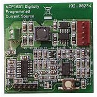
Manufacturer Part Number
MCP1631RD-MCC1
Description
REFERENCE DESIGN FOR MCP1631HV
Manufacturer
Microchip Technology
Type
Battery Managementr
Datasheets
1.MCP1631VHVT-330EST.pdf
(34 pages)
2.MCP1631HV-330EST.pdf
(54 pages)
3.MCP1631RD-MCC2.pdf
(20 pages)
4.MCP1631RD-MCC2.pdf
(328 pages)
5.MCP1631RD-MCC1.pdf
(28 pages)
Specifications of MCP1631RD-MCC1
Main Purpose
Power Management, Battery Charger
Embedded
Yes, MCU, 8-Bit
Utilized Ic / Part
MCP1631HV, PIC16F883
Primary Attributes
1 ~ 2 Cell- Li-Ion, 1 ~ 4 Cell- NiCd/NiMH
Secondary Attributes
Status LEDs
Supported Devices
MCP1631HV, PIC16F883 Device Type
Tool / Board Applications
Power Management-Battery Management
Development Tool Type
Reference Design
Input Voltage
5.5 V to 16 V
Product
Power Management Modules
Mcu Supported Families
MCP1631HV/PIC16F883 Family
Silicon Manufacturer
Microchip
Silicon Core Number
MCP1631HV
Kit Application Type
Reference Design
Application Sub Type
Battery Charger
Kit Contents
Board Only
Lead Free Status / RoHS Status
Lead free / RoHS Compliant
For Use With/related Products
MCP1631HV, PIC16F883
Lead Free Status / RoHS Status
Lead free / RoHS Compliant


EUSART ........................................................................... 151
F
Fail-Safe Clock Monitor....................................................... 71
Firmware Instructions........................................................ 231
Flash Program Memory .................................................... 111
Fuses. See Configuration Bits
G
General Call Address Support .......................................... 192
General Purpose Register File............................................ 22
I
I
I
I
I
© 2009 Microchip Technology Inc.
2
2
2
2
C (MSSP Module)
C Master Mode Reception.............................................. 198
C Master Mode Repeated Start Condition Timing.......... 197
C Module
Associated Registers
Asynchronous Mode ................................................. 153
Baud Rate Generator (BRG)
Synchronous Master Mode ............................... 171, 175
Synchronous Slave Mode
Fail-Safe Condition Clearing ....................................... 71
Fail-Safe Detection ..................................................... 71
Fail-Safe Operation..................................................... 71
Reset or Wake-up from Sleep..................................... 71
Writing....................................................................... 117
ACK Pulse......................................................... 189, 190
Addressing ................................................................ 190
Read/Write Bit Information (R/W Bit) ........................ 190
Reception.................................................................. 190
Serial Clock (RC3/SCK/SCL).................................... 190
Slave Mode ............................................................... 189
Transmission............................................................. 190
Acknowledge Sequence Timing................................ 201
Baud Rate Generator................................................ 195
Baud Rate Generator........................................ 163
12-bit Break Transmit and Receive .................. 169
Associated Registers
Auto-Wake-up on Break ................................... 168
Baud Rate Generator (BRG) ............................ 163
Clock Accuracy ................................................. 160
Receiver............................................................ 156
Setting up 9-bit Mode with Address Detect....... 158
Transmitter........................................................ 153
Auto Baud Rate Detect ..................................... 167
Baud Rate Error, Calculating ............................ 163
Baud Rates, Asynchronous Modes .................. 164
Formulas ........................................................... 163
High Baud Rate Select (BRGH Bit) .................. 163
Associated Registers
Reception.......................................................... 173
Requirements, Synchronous Receive .............. 266
Requirements, Synchronous Transmission ...... 266
Timing Diagram, Synchronous Receive ........... 266
Timing Diagram, Synchronous Transmission ... 266
Transmission .................................................... 171
Associated Registers
Reception.......................................................... 176
Transmission .................................................... 175
Receive..................................................... 159
Transmit.................................................... 155
Receive..................................................... 174
Transmit.................................................... 172
Receive..................................................... 176
Transmit.................................................... 175
PIC16F882/883/884/886/887
ID Locations...................................................................... 227
In-Circuit Debugger........................................................... 229
In-Circuit Serial Programming (ICSP)............................... 227
Indirect Addressing, INDF and FSR registers..................... 37
Instruction Format............................................................. 231
Instruction Set................................................................... 231
BRG Block Diagram ................................................. 195
BRG Reset Due to SDA Arbitration During
BRG Timing .............................................................. 195
Bus Collision
Bus Collision timing .................................................. 203
Clock Arbitration ....................................................... 202
Clock Arbitration Timing (Master Transmit) .............. 202
Effect of a Reset ....................................................... 202
General Call Address Support .................................. 192
Master Mode............................................................. 193
Master Mode 7-bit Reception Timing........................ 200
Master Mode Operation............................................ 194
Master Mode Start Condition Timing ........................ 196
Master Mode Support ............................................... 193
Master Mode Transmission ...................................... 198
Master Mode Transmit Sequence ............................ 194
Multi-Master Mode.................................................... 203
Repeat Start Condition Timing Waveform ................ 197
Sleep Operation........................................................ 202
Stop Condition Receive or Transmit Timing ............. 202
Stop Condition Timing .............................................. 201
Waveforms for 7-bit Reception ................................. 191
Waveforms for 7-bit Transmission............................ 191
ADDLW..................................................................... 233
ADDWF .................................................................... 233
ANDLW..................................................................... 233
ANDWF .................................................................... 233
BCF .......................................................................... 233
BSF........................................................................... 233
BTFSC...................................................................... 233
BTFSS ...................................................................... 234
CALL......................................................................... 234
CLRF ........................................................................ 234
CLRW ....................................................................... 234
CLRWDT .................................................................. 234
COMF ....................................................................... 234
DECF........................................................................ 234
DECFSZ ................................................................... 235
GOTO ....................................................................... 235
INCF ......................................................................... 235
INCFSZ..................................................................... 235
IORLW ...................................................................... 235
IORWF...................................................................... 235
MOVF ....................................................................... 236
MOVLW .................................................................... 236
MOVWF.................................................................... 236
NOP.......................................................................... 236
RETFIE..................................................................... 237
RETLW ..................................................................... 237
Start Condition.................................................. 205
Acknowledge .................................................... 203
Repeated Start Condition ................................. 206
Repeated Start Condition Timing (Case1)........ 206
Repeated Start Condition Timing (Case2)........ 206
Start Condition.................................................. 204
Start Condition Timing .............................. 204, 205
Stop Condition .................................................. 207
Stop Condition Timing (Case 1) ....................... 207
Stop Condition Timing (Case 2) ....................... 207
DS41291F-page 317
Related parts for MCP1631RD-MCC1
Image
Part Number
Description
Manufacturer
Datasheet
Request
R

Part Number:
Description:
REFERENCE DESIGN MCP1631HV
Manufacturer:
Microchip Technology
Datasheet:

Part Number:
Description:
REF DES BATT CHARG OR LED DRIVER
Manufacturer:
Microchip Technology
Datasheet:

Part Number:
Description:
Manufacturer:
Microchip Technology Inc.
Datasheet:
Part Number:
Description:
Manufacturer:
Microchip Technology Inc.
Datasheet:
Part Number:
Description:
Manufacturer:
Microchip Technology Inc.
Datasheet:
Part Number:
Description:
Manufacturer:
Microchip Technology Inc.
Datasheet:
Part Number:
Description:
Manufacturer:
Microchip Technology Inc.
Datasheet:
Part Number:
Description:
Manufacturer:
Microchip Technology Inc.
Datasheet:
Part Number:
Description:
Manufacturer:
Microchip Technology Inc.
Datasheet:
Part Number:
Description:
Manufacturer:
Microchip Technology Inc.
Datasheet: