MCP1631RD-MCC1 Microchip Technology, MCP1631RD-MCC1 Datasheet - Page 32
MCP1631RD-MCC1
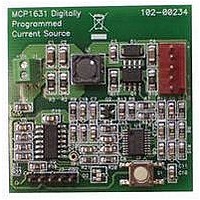
Manufacturer Part Number
MCP1631RD-MCC1
Description
REFERENCE DESIGN FOR MCP1631HV
Manufacturer
Microchip Technology
Type
Battery Managementr
Datasheets
1.MCP1631VHVT-330EST.pdf
(34 pages)
2.MCP1631HV-330EST.pdf
(54 pages)
3.MCP1631RD-MCC2.pdf
(20 pages)
4.MCP1631RD-MCC2.pdf
(328 pages)
5.MCP1631RD-MCC1.pdf
(28 pages)
Specifications of MCP1631RD-MCC1
Main Purpose
Power Management, Battery Charger
Embedded
Yes, MCU, 8-Bit
Utilized Ic / Part
MCP1631HV, PIC16F883
Primary Attributes
1 ~ 2 Cell- Li-Ion, 1 ~ 4 Cell- NiCd/NiMH
Secondary Attributes
Status LEDs
Supported Devices
MCP1631HV, PIC16F883 Device Type
Tool / Board Applications
Power Management-Battery Management
Development Tool Type
Reference Design
Input Voltage
5.5 V to 16 V
Product
Power Management Modules
Mcu Supported Families
MCP1631HV/PIC16F883 Family
Silicon Manufacturer
Microchip
Silicon Core Number
MCP1631HV
Kit Application Type
Reference Design
Application Sub Type
Battery Charger
Kit Contents
Board Only
Lead Free Status / RoHS Status
Lead free / RoHS Compliant
For Use With/related Products
MCP1631HV, PIC16F883
Lead Free Status / RoHS Status
Lead free / RoHS Compliant


PIC16F882/883/884/886/887
2.2.2.2
The OPTION register, shown in Register 2-2, is a
readable and writable register, which contains various
control bits to configure:
• Timer0/WDT prescaler
• External INT interrupt
• Timer0
• Weak pull-ups on PORTB
REGISTER 2-2:
DS41291F-page 30
bit 7
Legend:
R = Readable bit
-n = Value at POR
bit 7
bit 6
bit 5
bit 4
bit 3
bit 2-0
R/W-1
RBPU
OPTION Register
RBPU: PORTB Pull-up Enable bit
1 = PORTB pull-ups are disabled
0 = PORTB pull-ups are enabled by individual PORT latch values
INTEDG: Interrupt Edge Select bit
1 = Interrupt on rising edge of INT pin
0 = Interrupt on falling edge of INT pin
T0CS: Timer0 Clock Source Select bit
1 = Transition on T0CKI pin
0 = Internal instruction cycle clock (F
T0SE: Timer0 Source Edge Select bit
1 = Increment on high-to-low transition on T0CKI pin
0 = Increment on low-to-high transition on T0CKI pin
PSA: Prescaler Assignment bit
1 = Prescaler is assigned to the WDT
0 = Prescaler is assigned to the Timer0 module
PS<2:0>: Prescaler Rate Select bits
INTEDG
R/W-1
OPTION_REG: OPTION REGISTER
Bit Value
000
001
010
011
100
101
110
111
W = Writable bit
‘1’ = Bit is set
R/W-1
T0CS
Timer0 Rate
1 : 2
1 : 4
1 : 8
1 : 16
1 : 32
1 : 64
1 : 128
1 : 256
R/W-1
T0SE
WDT Rate
1 : 1
1 : 2
1 : 4
1 : 8
1 : 16
1 : 32
1 : 64
1 : 128
OSC
/4)
U = Unimplemented bit, read as ‘0’
‘0’ = Bit is cleared
R/W-1
PSA
Note:
To achieve a 1:1 prescaler assignment for
Timer0, assign the prescaler to the WDT by
setting PSA bit of the OPTION register to
‘1’. See Section 6.3 “Timer1 Prescaler”.
R/W-1
PS2
© 2009 Microchip Technology Inc.
x = Bit is unknown
R/W-1
PS1
R/W-1
PS0
bit 0
Related parts for MCP1631RD-MCC1
Image
Part Number
Description
Manufacturer
Datasheet
Request
R

Part Number:
Description:
REFERENCE DESIGN MCP1631HV
Manufacturer:
Microchip Technology
Datasheet:

Part Number:
Description:
REF DES BATT CHARG OR LED DRIVER
Manufacturer:
Microchip Technology
Datasheet:

Part Number:
Description:
Manufacturer:
Microchip Technology Inc.
Datasheet:
Part Number:
Description:
Manufacturer:
Microchip Technology Inc.
Datasheet:
Part Number:
Description:
Manufacturer:
Microchip Technology Inc.
Datasheet:
Part Number:
Description:
Manufacturer:
Microchip Technology Inc.
Datasheet:
Part Number:
Description:
Manufacturer:
Microchip Technology Inc.
Datasheet:
Part Number:
Description:
Manufacturer:
Microchip Technology Inc.
Datasheet:
Part Number:
Description:
Manufacturer:
Microchip Technology Inc.
Datasheet:
Part Number:
Description:
Manufacturer:
Microchip Technology Inc.
Datasheet: