NCP1271ADAPGEVB ON Semiconductor, NCP1271ADAPGEVB Datasheet - Page 12
NCP1271ADAPGEVB
Manufacturer Part Number
NCP1271ADAPGEVB
Description
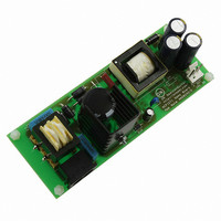
EVAL BOARD FOR NCP1271ADAPG
Manufacturer
ON Semiconductor
Datasheets
1.NCP1271P100G.pdf
(21 pages)
2.NCP1271ADAPGEVB.pdf
(1 pages)
3.NCP1271ADAPGEVB.pdf
(10 pages)
Specifications of NCP1271ADAPGEVB
Design Resources
NCP1271 Adapter EVB BOM NCP1271ADAPGEVB Gerber Files NCP1271EVB Schematic
Main Purpose
AC/DC, Primary Side
Outputs And Type
1, Isolated
Voltage - Output
19V
Current - Output
3A
Voltage - Input
85 ~ 265VAC
Regulator Topology
Flyback
Frequency - Switching
65kHz
Board Type
Fully Populated
Utilized Ic / Part
NCP1271
Silicon Manufacturer
On Semiconductor
Silicon Core Number
NCP1271
Kit Application Type
Power Management
Application Sub Type
PWM Controller
Peak Reflow Compatible (260 C)
No
Rohs Compliant
No
Lead Free Status / RoHS Status
Lead free / RoHS Compliant
Power - Output
-
Lead Free Status / Rohs Status
Lead free / RoHS Compliant
Other names
NCP1271ADAPGEVBOS


external components during a fault event. After the second
cycle, the controller tries to restart the application. If the
restart is not successful, then the process is repeated.
During this mode, V
reset level. Therefore, latched faults will not be cleared
unless the application is unplugged from the AC line (i.e.,
V
hiccup operation. Note that at each restart attempt, a soft
start is issued to minimize stress.
V
when the feedback pin is open (i.e. FB is greater than 3 V)
for 130 ms or V
Therefore, to take advantage of these features, the V
capacitor needs to be sized so that operation can be
maintained in the absence of the auxiliary winding for at
least 130 ms.
frequency with a 1 nF switch gate capacitance. Therefore,
to ensure at least 130 ms of operation, equation 1 can be
used to calculate that at least an 85 mF capacitor would be
necessary.
capacitance value needs to at least be large enough for the
output to charge up to a point where the auxiliary winding
can supply V
scenarios with different V
cap is too small, the application fails to start because the
bias supply voltage cannot be established before V
reduced to the V
12.6 V
9.1 V
5.8 V
t startup +
bulk
CC
Figure 25 shows a timing diagram of the V
As stated earlier, the NCP1271 enters a fault condition
The controller typically consumes 2.3 mA at a 65 kHz
If the 130 ms timer feature will not be used, then the
Figure 25. V
Capacitor
discharges).
Supply voltage, V
Drain current, I
C VCC DV
I CC1
CC
CC
CC(off)
CC
. Figure 26 describes different startup
Double Hiccup Operation in a Fault
drops below V
D
CC
+
CC
t startup
Condition
level.
85 mF · (12.6 V−9.1 V)
never drops below the 4 V latch
CC
capacitor values. If the V
Switching is missing in
every two V
featuring a “double−hiccup”
2.3 mA
CC(off)
CC
(9.1 V typical).
hiccup cycles
+ 130 ms
CC
double
http://onsemi.com
time
(eq. 1)
time
CC
CC
CC
is
12
close as possible to the V
to reduce switching noise. A small bypass capacitor on this
pin is also recommended. If the switching noise is large
enough, it could potentially cause V
and force a restart of the controller.
winding bias voltage and V
transient swings of the auxiliary winding are allowed. In
standby mode, the V
the low−frequency skip−cycle operation. The V
capacitor also affects this swing. Figure 27 illustrates the
possible swings.
12.6 V
12.6 V
9.1 V
0.6 V
9.1 V
5.8 V
0.6 V
It is highly recommended that the V
It is also recommended to have a margin between the
Figure 27. Timing Diagram of Standby Condition
Supply voltage, V
Drain current, I
Feedback pin voltage, V
Figure 26. Different Startup Scenarios of the
Output waveforms with a large enough V
Output waveforms with too small of a V
Circuits with Different V
D
CC
CC
t
startup
voltage swing can be higher due to
CC
FB
and ground pins of the product
CC(off)
CC
CC
Capacitors
so that all possible
to go below V
Desired level of V
CC
CC
capacitor be as
CC
capacitor
capacitor
time
time
time
V
V
CC
out
V
V
9.1 V
CC(off)
out
CC
V
time
time
skip
out
CC
Related parts for NCP1271ADAPGEVB
Image
Part Number
Description
Manufacturer
Datasheet
Request
R

Part Number:
Description:
ON Semiconductor [VOLTAGE REGULATOR]
Manufacturer:
ON Semiconductor
Datasheet:
Part Number:
Description:
357-036-542-201 CARDEDGE 36POS DL .156 BLK LOPRO
Manufacturer:
ON Semiconductor
Datasheet:
Part Number:
Description:
357-036-542-201 CARDEDGE 36POS DL .156 BLK LOPRO
Manufacturer:
ON Semiconductor
Datasheet:
Part Number:
Description:
357-036-542-201 CARDEDGE 36POS DL .156 BLK LOPRO
Manufacturer:
ON Semiconductor
Datasheet:
Part Number:
Description:
357-036-542-201 CARDEDGE 36POS DL .156 BLK LOPRO
Manufacturer:
ON Semiconductor
Datasheet:
Part Number:
Description:
357-036-542-201 CARDEDGE 36POS DL .156 BLK LOPRO
Manufacturer:
ON Semiconductor
Datasheet:
Part Number:
Description:
357-036-542-201 CARDEDGE 36POS DL .156 BLK LOPRO
Manufacturer:
ON Semiconductor
Datasheet:
Part Number:
Description:
357-036-542-201 CARDEDGE 36POS DL .156 BLK LOPRO
Manufacturer:
ON Semiconductor
Datasheet:
Part Number:
Description:
357-036-542-201 CARDEDGE 36POS DL .156 BLK LOPRO
Manufacturer:
ON Semiconductor
Datasheet:
Part Number:
Description:
357-036-542-201 CARDEDGE 36POS DL .156 BLK LOPRO
Manufacturer:
ON Semiconductor
Datasheet:
Part Number:
Description:
357-036-542-201 CARDEDGE 36POS DL .156 BLK LOPRO
Manufacturer:
ON Semiconductor
Datasheet:
Part Number:
Description:
Manufacturer:
ON Semiconductor
Datasheet:
Part Number:
Description:
Manufacturer:
ON Semiconductor
Datasheet:
Part Number:
Description:
Manufacturer:
ON Semiconductor
Datasheet: