NCP1271ADAPGEVB ON Semiconductor, NCP1271ADAPGEVB Datasheet - Page 16
NCP1271ADAPGEVB
Manufacturer Part Number
NCP1271ADAPGEVB
Description
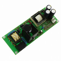
EVAL BOARD FOR NCP1271ADAPG
Manufacturer
ON Semiconductor
Datasheets
1.NCP1271P100G.pdf
(21 pages)
2.NCP1271ADAPGEVB.pdf
(1 pages)
3.NCP1271ADAPGEVB.pdf
(10 pages)
Specifications of NCP1271ADAPGEVB
Design Resources
NCP1271 Adapter EVB BOM NCP1271ADAPGEVB Gerber Files NCP1271EVB Schematic
Main Purpose
AC/DC, Primary Side
Outputs And Type
1, Isolated
Voltage - Output
19V
Current - Output
3A
Voltage - Input
85 ~ 265VAC
Regulator Topology
Flyback
Frequency - Switching
65kHz
Board Type
Fully Populated
Utilized Ic / Part
NCP1271
Silicon Manufacturer
On Semiconductor
Silicon Core Number
NCP1271
Kit Application Type
Power Management
Application Sub Type
PWM Controller
Peak Reflow Compatible (260 C)
No
Rohs Compliant
No
Lead Free Status / RoHS Status
Lead free / RoHS Compliant
Power - Output
-
Lead Free Status / Rohs Status
Lead free / RoHS Compliant
Other names
NCP1271ADAPGEVBOS


Recover from Standby
cycle operation, the circuit automatically disables the
normal Soft−Skip procedure and delivers maximum power
to the load (Figure 37). This feature, the Transient Load
Detector (TLD), is initiated anytime a skip event is exited
and the FB pin is greater than 2.85 V, as would be the case
for a sudden increase in output load.
External Latchoff Shutdown
V
V
above approximately 30 Vdc, then the HV FET ensure that
V
controller is reset by unplugging the power supply from the
wall and allowing V
the timing diagram of V
Skip/latch Pin (Pin 1) operation.
load current
Startup current source is
charging the V
output voltage
12.6 V
Startup current source turns
on when V
V FB
latch
CC
CC
5.8 V
In the event that a large load is encountered during skip
When the Skip/Latch input (Pin 1) is pulled higher than
Figure 39 defines the different voltage regions of the
I D
remains above V
1. When the voltage is above V
2. When the voltage is between V
drops below V
Figure 37. Transient Response from Standby
(8.0 V typical), the drive output is latched off until
8.7 V max), the circuit is in latchoff and all drive
pulses are disabled until V
(typical).
min, 6.5 V max) and V
Figure 38. Latchoff V
CC
CC
reaches 5.8 V
capacitor
CC(reset)
bulk
CC(latch)
CC
to discharge. Figure 38 illustrates
CC
in the latchoff condition.
(4.0 V
(5.8 V
CC
latch
Startup current source is
off when V
Timing Diagram
Maximum current available
CC
, the pin is considered
300 ms max
typical
when TLD level is hit
typical
latch
cycles below 4.0 V
skip−reset
). If Vbulk stays
CC
(7.1 V min,
). Therefore, the
is 12.6 V
(5.0 V
V TLD
V
skip
http://onsemi.com
16
implement different kinds of latching protection. The
NCP1271 applications note (AND8242/D) details several
simple circuits to implement overtemperature protection
(OTP) and overvoltage protection (OVP).
it is very important to put a noise decoupling capacitor
near Pin 1 to increase the noise immunity. It is also
recommended to always have a resistor from pin 1 to GND.
This further reduces the risk of premature latchoff. Also
note that if the additional latch−off circuitry has leakage,
it will modify the skip adjust setup.
External Non−Latched Shutdown
external non−latched shutdown can be easily implemented
by simply pulling FB below the skip level. This is an
inherent feature from the standby skip operation. Hence, it
allows the designer to implement additional non−latched
shutdown protection.
to GND (<190 mV). In addition to shutting off the output,
this method also places the part into a low current
consumption state.
The external latch feature allows the circuit designers to
In order to prevent unexpected latchoff due to noise,
Figure 40 illustrates the Feedback (pin 2) operation. An
The device can also be shutdown by pulling the V
3. When the voltage is between about 3.0 V and
4. When the voltage is between 0 V and 3.0 V, the
Figure 39. NCP1271 Pin 1 Operating Regions
to be opened. The skip level V
the default 1.2 V.
V
operating range of the feedback pin. Therefore,
the output does not switch.
V
feedback pin. Then the voltage on this pin sets
the skip level as explained earlier.
skip−reset
skip
V pin1
is within the operating range of the
Adjustable V
V
Output always low (skipped) here.
Output is latched off here.
Pin 1 considered to be opened.
skip
, the V
is reset to default level 1.2 V.
skip
skip
level is above the normal
range.
10 V (max limit)
0 V (no skip)
8V (V
5.7 V (V
3.0 V (always skip)
latch
skip−reset
skip
)
is restored to
)
CC
pin
Related parts for NCP1271ADAPGEVB
Image
Part Number
Description
Manufacturer
Datasheet
Request
R

Part Number:
Description:
ON Semiconductor [VOLTAGE REGULATOR]
Manufacturer:
ON Semiconductor
Datasheet:
Part Number:
Description:
357-036-542-201 CARDEDGE 36POS DL .156 BLK LOPRO
Manufacturer:
ON Semiconductor
Datasheet:
Part Number:
Description:
357-036-542-201 CARDEDGE 36POS DL .156 BLK LOPRO
Manufacturer:
ON Semiconductor
Datasheet:
Part Number:
Description:
357-036-542-201 CARDEDGE 36POS DL .156 BLK LOPRO
Manufacturer:
ON Semiconductor
Datasheet:
Part Number:
Description:
357-036-542-201 CARDEDGE 36POS DL .156 BLK LOPRO
Manufacturer:
ON Semiconductor
Datasheet:
Part Number:
Description:
357-036-542-201 CARDEDGE 36POS DL .156 BLK LOPRO
Manufacturer:
ON Semiconductor
Datasheet:
Part Number:
Description:
357-036-542-201 CARDEDGE 36POS DL .156 BLK LOPRO
Manufacturer:
ON Semiconductor
Datasheet:
Part Number:
Description:
357-036-542-201 CARDEDGE 36POS DL .156 BLK LOPRO
Manufacturer:
ON Semiconductor
Datasheet:
Part Number:
Description:
357-036-542-201 CARDEDGE 36POS DL .156 BLK LOPRO
Manufacturer:
ON Semiconductor
Datasheet:
Part Number:
Description:
357-036-542-201 CARDEDGE 36POS DL .156 BLK LOPRO
Manufacturer:
ON Semiconductor
Datasheet:
Part Number:
Description:
357-036-542-201 CARDEDGE 36POS DL .156 BLK LOPRO
Manufacturer:
ON Semiconductor
Datasheet:
Part Number:
Description:
Manufacturer:
ON Semiconductor
Datasheet:
Part Number:
Description:
Manufacturer:
ON Semiconductor
Datasheet:
Part Number:
Description:
Manufacturer:
ON Semiconductor
Datasheet: