NCP1271ADAPGEVB ON Semiconductor, NCP1271ADAPGEVB Datasheet - Page 13
NCP1271ADAPGEVB
Manufacturer Part Number
NCP1271ADAPGEVB
Description
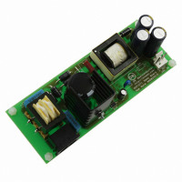
EVAL BOARD FOR NCP1271ADAPG
Manufacturer
ON Semiconductor
Datasheets
1.NCP1271P100G.pdf
(21 pages)
2.NCP1271ADAPGEVB.pdf
(1 pages)
3.NCP1271ADAPGEVB.pdf
(10 pages)
Specifications of NCP1271ADAPGEVB
Design Resources
NCP1271 Adapter EVB BOM NCP1271ADAPGEVB Gerber Files NCP1271EVB Schematic
Main Purpose
AC/DC, Primary Side
Outputs And Type
1, Isolated
Voltage - Output
19V
Current - Output
3A
Voltage - Input
85 ~ 265VAC
Regulator Topology
Flyback
Frequency - Switching
65kHz
Board Type
Fully Populated
Utilized Ic / Part
NCP1271
Silicon Manufacturer
On Semiconductor
Silicon Core Number
NCP1271
Kit Application Type
Power Management
Application Sub Type
PWM Controller
Peak Reflow Compatible (260 C)
No
Rohs Compliant
No
Lead Free Status / RoHS Status
Lead free / RoHS Compliant
Power - Output
-
Lead Free Status / Rohs Status
Lead free / RoHS Compliant
Other names
NCP1271ADAPGEVBOS


Soft−Start Operation
included
comparator. When the NCP1271 starts up, a soft−start
voltage V
to 1.0 V in 4.0 ms and stays at 1.0 V afterward. This voltage
V
voltage (V
modulation voltage V
generation. Initially, (V
output voltage is low. As a result, V
soft start function and slowly ramps up the duty cycle (and
therefore the primary current) for the initial 4.0 ms. This
provides a greatly reduced stress on the power devices
during startup.
SS
Figures 28 and 29 show how the soft−start feature is
Figure 28. V
Figure 29. Soft−Start (Time = 0 at V
is compared with the divided−by−3 feedback pin
4 ms
4 ms
4 ms
Soft−start voltage, V
Feedback pin voltage divided−by−3, V
Pulse Width Modulation voltage, V
Drain Current, I
time must be less than130 ms
to prevent fault condition
SS
FB
in
begins at 0 V. V
V
/3). The lesser of V
FB
V
the
/ 3
SS
PWM
D
0
is the lesser of V
pulse−width
SS
FB
PWM
/3) is above 1.0 V because the
1
SS
+
−
increases gradually from 0 V
in the PWM duty cycle
SS
and (V
PWM
PWM
modulation
1 V
V
SS
FB
FB
PWM
CC
/3
is limited by the
and (V
/3) becomes the
= V
1 V
CC(on)
FB
(PWM)
/3)
http://onsemi.com
time
time
time
time
1 V
)
13
Current−Mode Pulse−Width Modulation
PWM with internal ramp compensation. A pair of current
sense resistors R
current I
inductor and current sense resistor, a corresponding voltage
ramp is placed on the CS pin (pin 3). This voltage ranges
from very low to as high as the modulation voltage V
(maximum of 1.0 V) before turning the drive off. If the
internal current ramp is ignored (i.e., R
maximum possible drain current I
Equation 2. This sets the primary current limit on a cycle
by cycle basis.
internal clock turns the Drive Output (Pin 5) high in each
switching cycle. The Drive Output goes low when the CS
(Pin 3) voltage V
V
maximum duty cycle is limited to 80% (typically) in the
output RS latch.
PWM
Output
PWM
The NCP1271 uses a current−mode fixed−frequency
The timing diagram of the PWM is in Figure 31. An
. This generates the pulse width (or duty cycle). The
Figure 31. Current−Mode Timing Diagram
Figure 30. Current−Mode Implementation
D
. As the drain current ramps up through the
80%
max duty
Q
R
S
CS
Clock
CS
intersects with the modulation voltage
I D(max) +
and R
+
−
(1V max. signal)
V
PWM
ramp
180ns
LEB
I
ramp
R CS
1 V
sense the flyback drain
V
1
CS
D(max)
0
ramp
3
PWM
Output
V
clock
CS
CS
≈ 0) then the
is shown in
V
R
PWM
ramp
V
(eq. 2)
bulk
R
PWM
I D
CS
Related parts for NCP1271ADAPGEVB
Image
Part Number
Description
Manufacturer
Datasheet
Request
R

Part Number:
Description:
ON Semiconductor [VOLTAGE REGULATOR]
Manufacturer:
ON Semiconductor
Datasheet:
Part Number:
Description:
357-036-542-201 CARDEDGE 36POS DL .156 BLK LOPRO
Manufacturer:
ON Semiconductor
Datasheet:
Part Number:
Description:
357-036-542-201 CARDEDGE 36POS DL .156 BLK LOPRO
Manufacturer:
ON Semiconductor
Datasheet:
Part Number:
Description:
357-036-542-201 CARDEDGE 36POS DL .156 BLK LOPRO
Manufacturer:
ON Semiconductor
Datasheet:
Part Number:
Description:
357-036-542-201 CARDEDGE 36POS DL .156 BLK LOPRO
Manufacturer:
ON Semiconductor
Datasheet:
Part Number:
Description:
357-036-542-201 CARDEDGE 36POS DL .156 BLK LOPRO
Manufacturer:
ON Semiconductor
Datasheet:
Part Number:
Description:
357-036-542-201 CARDEDGE 36POS DL .156 BLK LOPRO
Manufacturer:
ON Semiconductor
Datasheet:
Part Number:
Description:
357-036-542-201 CARDEDGE 36POS DL .156 BLK LOPRO
Manufacturer:
ON Semiconductor
Datasheet:
Part Number:
Description:
357-036-542-201 CARDEDGE 36POS DL .156 BLK LOPRO
Manufacturer:
ON Semiconductor
Datasheet:
Part Number:
Description:
357-036-542-201 CARDEDGE 36POS DL .156 BLK LOPRO
Manufacturer:
ON Semiconductor
Datasheet:
Part Number:
Description:
357-036-542-201 CARDEDGE 36POS DL .156 BLK LOPRO
Manufacturer:
ON Semiconductor
Datasheet:
Part Number:
Description:
Manufacturer:
ON Semiconductor
Datasheet:
Part Number:
Description:
Manufacturer:
ON Semiconductor
Datasheet:
Part Number:
Description:
Manufacturer:
ON Semiconductor
Datasheet: