EVL130W-STRLIG STMicroelectronics, EVL130W-STRLIG Datasheet - Page 6
EVL130W-STRLIG
Manufacturer Part Number
EVL130W-STRLIG
Description
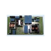
BOARD EVAL L6562AT L6599AT
Manufacturer
STMicroelectronics
Specifications of EVL130W-STRLIG
Current - Output / Channel
2.7A
Outputs And Type
1, Isolated
Voltage - Output
48V
Features
EN55022 class B compliant
Voltage - Input
85 ~ 305 V
Utilized Ic / Part
L6562AT, L6599AT
Description/function
SMPS for LED Street Lighting Applications
Data Bus Width
4 bit
Maximum Clock Frequency
30 MHz
Maximum Power Dissipation
130 W
Operating Supply Voltage
85 V to 305 V
Operating Voltage
48 V
Product
Display Modules
Lead Free Status / RoHS Status
Lead free / RoHS Compliant
For Use With/related Products
L6562AT, L6599AT
Other names
497-10541
Available stocks
Company
Part Number
Manufacturer
Quantity
Price


Main characteristics and circuit description
1
1.1
6/35
Main characteristics and circuit description
The main features of the SMPS are listed here below:
●
●
●
●
●
●
●
●
●
Power Factor corrector
The PFC stage, working in transition mode, acts as a preregulator and powers the resonant
stage with the output voltage of 450 V. The PFC power topology is a conventional boost
converter, connected to the output of the rectifier bridge D3. It is completed by the coil L1,
manufactured by MAGNETICA, the diode D2 and the capacitors C5, C6 and C7 in parallel.
The PFC output capacitors are film type, 5 µF - 800 V manufactured by EPCOS. Using film
capacitors to replace the typical electrolytic capacitors allows increasing considerably the
MTBF of the board.
The boost switch is represented by the power MOSFET Q2. The board is equipped with an
input EMI filter necessary to filter the commutation noise coming from the boost stage. The
PFC implements the controller L6562AT, a small and inexpensive controller that is
guaranteed for operation over a wide temperature range.
At startup, the L6562AT is supplied by the startup resistors R5, R8, R13 charging the
capacitor C13. Once the PFC begins switching, a charge pump connected to the auxiliary
winding of the PFC inductor L1 supplies both PFC and resonant controllers via a small
linear regulator implemented by Q1. Once both stages have been activated, the controllers
are supplied also by the auxiliary winding of the resonant transformer, assuring correct
supply voltage during operation of all load conditions. The L1 auxiliary winding is also
connected to the L6562AT pin #5 (ZCD) through the resistor R18. Its purpose is to provide
the information that L1 has demagnetized, needed by the internal logic for triggering a new
switching cycle. The PFC boost peak current is sensed by resistors R33 and R34 in series
to the MOSFET source. The signal is fed into pin #4 (CS) of the L6562AT, via the filter R27
and C16.
The divider R7, R12, R14 and R22 provides the L6562AT multiplier with the information of
the instantaneous mains voltage that is used to modulate the peak current of the boost.
The resistors R2, R6, R9 with R15 and R16 are dedicated to sense the output voltage and
feed to the L6562AT the feedback information necessary to maintain the output voltage
regulated. The components C11, R20 and C12 constitute the error amplifier compensation
network necessary to keep the required loop stability.
Extended input mains range: 85 ÷ 305 V
Output voltage: 48 V at 2.7 A
Long-life, electrolytic capacitors are not used
Mains harmonics: acc. to EN61000-3-2 Class-C
Efficiency at full load: better than 90% at 115 V
EMI: according to EN55022-Class-B, EN55015
Safety: double insulation, according to EN60950, SELV
Dimensions: 75 x 135 mm, 30 mm components maximum height
PCB: single side, 35 µm, FR-4, mixed PTH/SMT
Doc ID 16775 Rev 1
AC
- frequency 45 ÷ 55 Hz
AC
AN3106
Related parts for EVL130W-STRLIG
Image
Part Number
Description
Manufacturer
Datasheet
Request
R

Part Number:
Description:
BOARD EVAL L6562AT L6599AT
Manufacturer:
STMicroelectronics
Datasheet:
Part Number:
Description:
STMicroelectronics [RIPPLE-CARRY BINARY COUNTER/DIVIDERS]
Manufacturer:
STMicroelectronics
Datasheet:
Part Number:
Description:
STMicroelectronics [LIQUID-CRYSTAL DISPLAY DRIVERS]
Manufacturer:
STMicroelectronics
Datasheet:

Part Number:
Description:
BOARD EVAL FOR MEMS SENSORS
Manufacturer:
STMicroelectronics
Datasheet:
Part Number:
Description:
NPN TRANSISTOR POWER MODULE
Manufacturer:
STMicroelectronics
Datasheet:
Part Number:
Description:
TURBOSWITCH ULTRA-FAST HIGH VOLTAGE DIODE
Manufacturer:
STMicroelectronics
Datasheet:
Part Number:
Description:
Manufacturer:
STMicroelectronics
Datasheet:
Part Number:
Description:
DIODE / SCR MODULE
Manufacturer:
STMicroelectronics
Datasheet:
Part Number:
Description:
DIODE / SCR MODULE
Manufacturer:
STMicroelectronics
Datasheet:
Part Number:
Description:
Search -----> STE16N100
Manufacturer:
STMicroelectronics
Datasheet:
Part Number:
Description:
Search ---> STE53NA50
Manufacturer:
STMicroelectronics
Datasheet:
Part Number:
Description:
NPN Transistor Power Module
Manufacturer:
STMicroelectronics
Datasheet: