MCP651EV-VOS Microchip Technology, MCP651EV-VOS Datasheet - Page 10
MCP651EV-VOS
Manufacturer Part Number
MCP651EV-VOS
Description
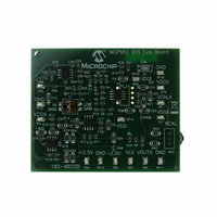
BOARD EVAL OP AMP MCP651
Manufacturer
Microchip Technology
Series
mCal Technologyr
Specifications of MCP651EV-VOS
Channels Per Ic
1 - Single
Amplifier Type
General Purpose
Output Type
Single-Ended, Rail-to-Rail
Slew Rate
30 V/µs
Current - Output / Channel
100mA
Operating Temperature
-40°C ~ 125°C
Current - Supply (main Ic)
6mA
Voltage - Supply, Single/dual (±)
2.5 V ~ 5.5 V
Board Type
Fully Populated
Utilized Ic / Part
MCP651
Processor To Be Evaluated
MCP651
Maximum Operating Temperature
+ 125 C
Minimum Operating Temperature
- 40 C
Operating Supply Voltage
2.5 V to 5.5 V
Tool Type
Evaluation Board
Core Architecture
PIC
Cpu Core
PIC
Data Bus Width
8 bit
Lead Free Status / RoHS Status
Lead free / RoHS Compliant
-3db Bandwidth
-
Lead Free Status / Rohs Status
Lead free / RoHS Compliant
Available stocks
Company
Part Number
Manufacturer
Quantity
Price
Company:

Part Number:
MCP651EV-VOS
Manufacturer:
Microchip Technology
Quantity:
135
Company:
Part Number:
MCP651EV-VOS
Manufacturer:
MICROCHIP
Quantity:
12 000


1.3
1.4
DS51834A-page 6
INTENDED USE
DESCRIPTION
The MCP651 Input Offset Evaluation Board is intended to provide a simple means to
measure the MCP651 Input Offset Evaluation Board op amp’s input offset voltage
under a variety of operating conditions. The measured input offset voltage (V
includes the input offset voltage specified in the data sheet (V
power supply voltage (PSRR), common mode voltage (CMRR), output voltage (A
input offset voltage drift over temperature (ΔV
The MCP651 Input Offset Evaluation Board works most effectively at room tempera-
ture (near 25°C). Measurements at other temperatures should be done in an oven
where the air velocity is minimal.
This section starts with the conversion of DUT bias voltages described in the MCP651
data sheet to the voltages on this board. Then there is a discussion of the circuitry that
controls the DUT’s output voltage (V
(V
details of this board are given in Appendix A. “Schematics and Layouts” and
Appendix B. “Bill Of Materials (BOM)”.
1.4.1
The MCP651 data sheet describes all of its bias voltages relative to V
assumed to be at ground (0V). On the other hand, the MCP651 Input Offset Evaluation
Board sets the DUT’s input common mode voltage to 0V. The user needs to convert
from the first set of voltages to the second set (by subtracting V
TABLE 1-1:
The supply voltages V
quiescent current (I
EQUATION 1-1:
Data Sheet Bias Voltage
OST
). Finally, other portions of the circuit, and their purpose, are discussed. Complete
Conversion of Bias Voltages
V
V
V
V
V
(V)
OUT
V
CAL
CM
DD
SS
L
CONVERSION OF BIAS VOLTAGES
Q
= 6 mA):
DDX
V
V
DDX
SSX
and V
Conversion Equations
=
=
V
V
SSX
SSI
DDI
V
V
V
V
V
V
OUT
CAL
CM
DD
–
SS
OUTX
L
can be estimated using the MCP651’s typical
+
I
– V
Q
– V
– V
– V
– V
I
– V
(
Q
10
CM
(
) and amplifies its total input offset voltage
CM
CM
CM
10
CM
CM
Ω
)
Ω
≈
OS
)
V
≈
/ΔT
SSI
V
DDI
–
A
) and 1/f noise.
60 mV
+
Evaluation Board Bias Voltage
60 mV
© 2009 Microchip Technology Inc.
OS
) plus changes due to:
CM
V
CMX
V
V
):
V
V
V
OUTX
CALX
(V)
DDI
SSI
LX
= 0V
SS
, which is
OST
)
OL
),
Related parts for MCP651EV-VOS
Image
Part Number
Description
Manufacturer
Datasheet
Request
R

Part Number:
Description:
Manufacturer:
Microchip Technology Inc.
Datasheet:
Part Number:
Description:
Manufacturer:
Microchip Technology Inc.
Datasheet:
Part Number:
Description:
Manufacturer:
Microchip Technology Inc.
Datasheet:
Part Number:
Description:
Manufacturer:
Microchip Technology Inc.
Datasheet:
Part Number:
Description:
Manufacturer:
Microchip Technology Inc.
Datasheet:
Part Number:
Description:
Manufacturer:
Microchip Technology Inc.
Datasheet:
Part Number:
Description:
Manufacturer:
Microchip Technology Inc.
Datasheet:
Part Number:
Description:
Manufacturer:
Microchip Technology Inc.
Datasheet: