MCP651EV-VOS Microchip Technology, MCP651EV-VOS Datasheet - Page 13
MCP651EV-VOS
Manufacturer Part Number
MCP651EV-VOS
Description
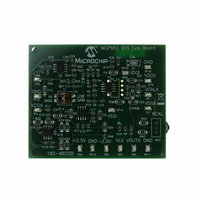
BOARD EVAL OP AMP MCP651
Manufacturer
Microchip Technology
Series
mCal Technologyr
Specifications of MCP651EV-VOS
Channels Per Ic
1 - Single
Amplifier Type
General Purpose
Output Type
Single-Ended, Rail-to-Rail
Slew Rate
30 V/µs
Current - Output / Channel
100mA
Operating Temperature
-40°C ~ 125°C
Current - Supply (main Ic)
6mA
Voltage - Supply, Single/dual (±)
2.5 V ~ 5.5 V
Board Type
Fully Populated
Utilized Ic / Part
MCP651
Processor To Be Evaluated
MCP651
Maximum Operating Temperature
+ 125 C
Minimum Operating Temperature
- 40 C
Operating Supply Voltage
2.5 V to 5.5 V
Tool Type
Evaluation Board
Core Architecture
PIC
Cpu Core
PIC
Data Bus Width
8 bit
Lead Free Status / RoHS Status
Lead free / RoHS Compliant
-3db Bandwidth
-
Lead Free Status / Rohs Status
Lead free / RoHS Compliant
Available stocks
Company
Part Number
Manufacturer
Quantity
Price
Company:

Part Number:
MCP651EV-VOS
Manufacturer:
Microchip Technology
Quantity:
135
Company:
Part Number:
MCP651EV-VOS
Manufacturer:
MICROCHIP
Quantity:
12 000


© 2009 Microchip Technology Inc.
1.4.3
Figure 1-3 shows the basic DUT biasing circuitry, except the input pins which have
already been discussed (V
FIGURE 1-3:
Lab power supplies are connected to V
R
op amps on the board. Since the MCP651’s quiescent current is between 3 mA and
9 mA, the actual power supply voltages (V
90 mV. I
EQUATION 1-3:
The DUT’s V
when it is in calibration mode. Thus, the DUT’s offset (V
this board) is equal to V
The RCAL potentiometer (POT or R43), with the resistors R
The values chosen allow the POT to cover the specified V
Connecting a voltmeter to V
that it is also possible to drive V
be, but doesn’t have to be, at mid-range).
V
control loop. If V
railed at the corresponding supply voltage.
The load resistor (R
usually set to mid-supply. The V
loading on V
OUTX
38
, along with the capacitors C
is set, as previously explained, to be equal to V
DD
V
DUT Bias Voltage Inputs
V
V
and I
CALX
DDX
OUTX
SSX
CAL
COX
SS
pin sets its internal common mode voltage (V
(about 40 kΩ).
4.49Ω
4.49Ω
2.2 kΩ
can be calculated as (I
L
10 kΩ
R
R
DUT Bias Circuitry.
150Ω
is at or beyond V
or R
37
38
R
R
R
44
43
42
CALX
10
CMX
CALX
) is biased to the externally supplied voltage V
.
CALX
= 0V).
13
C
10 µF
C
10 µF
LX
, C
makes it possible to set the POT accurately. Notice
21
22
4.49Ω
4.49Ω
I
DD
C
100 nF
connection can be left open, which minimizes the
R
R
I
SS
14
29
25
30
with an external voltage source (the wiper should
=
SSI
, C
=
DDX
V
-------------------------------- -
V
----------------------------
21
or V
DDX
C
100 nF
C
100 nF
SSX
DDI
SS
and V
13
14
and C
10
10
DUT
V
is negative):
–
DDI
–
and V
Ω
CAL
Ω
V
V
V
V
SSI
DDI
, then the loop forces V
DD
SS
SSX
22
V
OUT
, minimize crosstalk from the other
I
I
SSI
DD
U
SS
. The resistors R
V
V
1
DDI
SSI
COX
OS
) are different by 30 mV to
CALX
) is small when V
by the integrator in the PI
42
R
1.00 kΩ
10
range, and a little more.
CMX
and R
of the MCP651)
43
29
V
V
, sets V
OUTX
LX
DS51834A-page 9
, R
OUTX
30
LX
CMX
, R
. V
to be
CALX
(0V on
37
LX
and
is
.
Related parts for MCP651EV-VOS
Image
Part Number
Description
Manufacturer
Datasheet
Request
R

Part Number:
Description:
Manufacturer:
Microchip Technology Inc.
Datasheet:
Part Number:
Description:
Manufacturer:
Microchip Technology Inc.
Datasheet:
Part Number:
Description:
Manufacturer:
Microchip Technology Inc.
Datasheet:
Part Number:
Description:
Manufacturer:
Microchip Technology Inc.
Datasheet:
Part Number:
Description:
Manufacturer:
Microchip Technology Inc.
Datasheet:
Part Number:
Description:
Manufacturer:
Microchip Technology Inc.
Datasheet:
Part Number:
Description:
Manufacturer:
Microchip Technology Inc.
Datasheet:
Part Number:
Description:
Manufacturer:
Microchip Technology Inc.
Datasheet: