MCP651EV-VOS Microchip Technology, MCP651EV-VOS Datasheet - Page 12
MCP651EV-VOS
Manufacturer Part Number
MCP651EV-VOS
Description
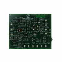
BOARD EVAL OP AMP MCP651
Manufacturer
Microchip Technology
Series
mCal Technologyr
Specifications of MCP651EV-VOS
Channels Per Ic
1 - Single
Amplifier Type
General Purpose
Output Type
Single-Ended, Rail-to-Rail
Slew Rate
30 V/µs
Current - Output / Channel
100mA
Operating Temperature
-40°C ~ 125°C
Current - Supply (main Ic)
6mA
Voltage - Supply, Single/dual (±)
2.5 V ~ 5.5 V
Board Type
Fully Populated
Utilized Ic / Part
MCP651
Processor To Be Evaluated
MCP651
Maximum Operating Temperature
+ 125 C
Minimum Operating Temperature
- 40 C
Operating Supply Voltage
2.5 V to 5.5 V
Tool Type
Evaluation Board
Core Architecture
PIC
Cpu Core
PIC
Data Bus Width
8 bit
Lead Free Status / RoHS Status
Lead free / RoHS Compliant
-3db Bandwidth
-
Lead Free Status / Rohs Status
Lead free / RoHS Compliant
Available stocks
Company
Part Number
Manufacturer
Quantity
Price
Company:

Part Number:
MCP651EV-VOS
Manufacturer:
Microchip Technology
Quantity:
135
Company:
Part Number:
MCP651EV-VOS
Manufacturer:
MICROCHIP
Quantity:
12 000


DS51834A-page 8
Analysis of this simplified circuit gives the following nominal circuit outputs:
EQUATION 1-2:
R
are oriented on the Printed Circuit Board (PCB) to cancel their thermoelectric voltages.
The parallel resistances R
DUT’s input bias currents to the measured V
affect V
V
The unity gain buffer (+1 gain on the bottom right) isolates the V
the following attenuator and integrator. Although it’s not shown here, the resistor R14
at the input to the “+1 Buffer” ensures its output voltage is 0V when the V
is left open.
The attenuators (1/G
U2 and U3 (“+1 Buffer” and (“Integrator”). For instance, when V
V
1.80V.
The differential integrator accumulates the scaled difference between V
V
Resistor R
R
A proportional term (the P part of the PI controller) is also injected at the DUT’s input
through resistor R
negligible above 16 Hz). It also sets a low frequency DUT noise gain of about 505 V/V.
This proportional term is rolled off by C
interact with the integrator term, and low enough to keep the DUT stable. Thus, C
minimizes noise gain at higher frequencies, which reduces the chance of unwanted
feedback effects.
With the overall gain G
V
distinguish steps of either 5 µV or 0.5 µV, respectively.
The DUT’s noise seen at the input to G
R
Lowpass Filter (f
The measured noise, over a 140 second period of time with a typical part, was about
19 µV
V
OST
SSI
OUTX
OST
OS
Where:
1
3
78
; it minimizes the error at V
and R
and C
specification (±200 µV, maximum at +25°C).
=0.3V and V
of ±0.02 µV.
values up to either ±12.4 mV or ±1.25 mV. A voltmeter with 1 mV resolution can
G
P-P
, which slowly forces this difference to zero (the I part of the PI controller).
A
M
G
G
); the typical value of I
2
referred to input (RTI). This compares favorably with the MCP651’s calibrated
M
2
A
56
(R
(0.28 kHz). This implies that this noise is dominated by the 1/f noise. The
injects the integrator’s output at the DUT’s input through resistors R
= 1 + R4/R3 ≈ 51.00 V/V
≈ 201.0 V/V, S2 (position 1) closed
≈ 1998 V/V, S2 (position 1) open
12
) balance the circuit at the DUT’s input. These resistors are small, and
BW
DDI
78
≈ 1.6 Hz) reduces this 1/f noise a little more before it is seen at V
; it stabilizes the control loop (the integrator term becomes
INT
= 5.8V), the voltages at the outputs of the attenuators (1/G
A
) scale V
G
1
M
||R
of either 201 V/V or 1998 V/V, this circuit can measure
2
OUTX
and R
OS
COX
at +125°C is ±100 pA, which produces a change in
.
V
V
OUTX
M
and V
3
||R
≈
2
M
G
starting at 0.18 kHz; this is high enough to not
4
has a noise power bandwidth (NPBW) set by
≈
A
G
are equal to minimize the contribution of the
OUTX
V
OST
M
COX
V
OST
(contributions by R
so that they do not overdrive op amps
© 2009 Microchip Technology Inc.
OUTX
COX
5
through R
input filters from
= 5.6V (given
COX
COX
connector
and
8
do not
INT
4
and
2
) is
M
.
Related parts for MCP651EV-VOS
Image
Part Number
Description
Manufacturer
Datasheet
Request
R

Part Number:
Description:
Manufacturer:
Microchip Technology Inc.
Datasheet:
Part Number:
Description:
Manufacturer:
Microchip Technology Inc.
Datasheet:
Part Number:
Description:
Manufacturer:
Microchip Technology Inc.
Datasheet:
Part Number:
Description:
Manufacturer:
Microchip Technology Inc.
Datasheet:
Part Number:
Description:
Manufacturer:
Microchip Technology Inc.
Datasheet:
Part Number:
Description:
Manufacturer:
Microchip Technology Inc.
Datasheet:
Part Number:
Description:
Manufacturer:
Microchip Technology Inc.
Datasheet:
Part Number:
Description:
Manufacturer:
Microchip Technology Inc.
Datasheet: