MCP651EV-VOS Microchip Technology, MCP651EV-VOS Datasheet - Page 18
MCP651EV-VOS
Manufacturer Part Number
MCP651EV-VOS
Description
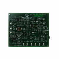
BOARD EVAL OP AMP MCP651
Manufacturer
Microchip Technology
Series
mCal Technologyr
Specifications of MCP651EV-VOS
Channels Per Ic
1 - Single
Amplifier Type
General Purpose
Output Type
Single-Ended, Rail-to-Rail
Slew Rate
30 V/µs
Current - Output / Channel
100mA
Operating Temperature
-40°C ~ 125°C
Current - Supply (main Ic)
6mA
Voltage - Supply, Single/dual (±)
2.5 V ~ 5.5 V
Board Type
Fully Populated
Utilized Ic / Part
MCP651
Processor To Be Evaluated
MCP651
Maximum Operating Temperature
+ 125 C
Minimum Operating Temperature
- 40 C
Operating Supply Voltage
2.5 V to 5.5 V
Tool Type
Evaluation Board
Core Architecture
PIC
Cpu Core
PIC
Data Bus Width
8 bit
Lead Free Status / RoHS Status
Lead free / RoHS Compliant
-3db Bandwidth
-
Lead Free Status / Rohs Status
Lead free / RoHS Compliant
Available stocks
Company
Part Number
Manufacturer
Quantity
Price
Company:

Part Number:
MCP651EV-VOS
Manufacturer:
Microchip Technology
Quantity:
135
Company:
Part Number:
MCP651EV-VOS
Manufacturer:
MICROCHIP
Quantity:
12 000


2.4
DS51834A-page 14
OPERATING CONDITIONS
The MCP651 Input Offset Evaluation Board works most effectively at room
temperature (near 25°C). Measurements at other temperatures should be done in an
oven where the air velocity is minimal. Table 2-1 shows the various DUT voltages (as
described in the data sheet), their nominal values and ranges, and how to convert to
the voltages needed on the MCP651 Input Offset Evaluation Board.
TABLE 2-1:
Once the MCP651 Input Offset Evaluation Board is powered up, the switches can be
set for the desired operation. S1 (a normally off push-button switch) starts a calibration
event (CAL), internal to the DUT, when pushed. S2 (top position) sets the gain of the
amplifier (G
TABLE 2-2:
The gain is usually set low. It can be set high just after a calibration event, before
changing the DUT’s bias point, to obtain more accurate results for the calibrated offset
voltage.
The POT (R
input voltage set during a calibration event (initiated by pushing S1). Adjusting this POT
does not have an effect on the circuit’s behavior until the CAL switch (S1) is pushed.
V
V
V
V
V
V
CAL/CS
Note 1:
DD
SS
CM
OUT
L
CAL
Switch
Data Sheet
Symbol
S1
S2
(Note 2)
2:
3:
4:
5:
At T
Set the desired V
be the same voltage.
When the V
connected, so V
The circuit forces CAL/CS to stay within its range (as long as the supply voltages
are constant when the CAL switch is activated). Normally, the part is on.
These numbers are for the MCP651 op amp.
M
CAL
No Input
Pushed
Top Switch to the left
Top Switch to the right
(Bottom Switch)
) either high or low. See Table 2-2 for details.
A
= +25°C. See the data sheet for changes in V
or R
CONVERTING VOLTAGES FOR THE BOARD
SWITCH OPERATION
Single Supply Voltages (V)
2.5 or 5.5
0
V
V
V
V
V
DD
DD
DD
DD
SS
43
CAL
/3
/2
/2
/3 (Note 3)
Nominal
) adjusts V
pin left open. However, this board always has the POT (R43)
CALX
OUT
Input
is never truly open.
voltage at the V
CALX
2.5 to 5.5
0
V
(Note 1)
V
V
V
V
SS
SS
SS
SS
SS
. This voltage is where the DUT’s common mode
– 0.3 to V
+ 0.2 to V
to V
+ 0.1 to V
to V
DD
DD
Range
COX
Normal Operation
Calibration event started in DUT
High Gain (1998 V/V)
Low Gain (201 V/V)
(Don’t Care)
DD
DD
DD
input; the integrator then forces V
– 1.3
– 0.2
– 1.4
CM
© 2009 Microchip Technology Inc.
range vs. T
V
V
0
V
V
V
(Note 4)
DDX
SSX
OUTX
LX
CALX
Result
Equations (V)
Conversion
← V
← V
← V
← V
← V
← V
A
.
DD
SS
CM
OUT
L
CAL
– V
– V
– V
– V
– V
– V
CM
CM
CM
CM
OUT
CM
CM
to
Related parts for MCP651EV-VOS
Image
Part Number
Description
Manufacturer
Datasheet
Request
R

Part Number:
Description:
Manufacturer:
Microchip Technology Inc.
Datasheet:
Part Number:
Description:
Manufacturer:
Microchip Technology Inc.
Datasheet:
Part Number:
Description:
Manufacturer:
Microchip Technology Inc.
Datasheet:
Part Number:
Description:
Manufacturer:
Microchip Technology Inc.
Datasheet:
Part Number:
Description:
Manufacturer:
Microchip Technology Inc.
Datasheet:
Part Number:
Description:
Manufacturer:
Microchip Technology Inc.
Datasheet:
Part Number:
Description:
Manufacturer:
Microchip Technology Inc.
Datasheet:
Part Number:
Description:
Manufacturer:
Microchip Technology Inc.
Datasheet: