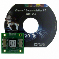
ADIS16240/PCBZ Analog Devices Inc, ADIS16240/PCBZ Datasheet

ADIS16240/PCBZ
Specifications of ADIS16240/PCBZ
Related parts for ADIS16240/PCBZ
ADIS16240/PCBZ Summary of contents
Page 1
FEATURES Digital triple-axis accelerometer, ±19 g Programmable event recorder Internal and external trigger inputs Low power operation Sleep mode current: 100 μA Continuous sampling current: 1 mA, 1 kSPS Wake-up and record function External trigger input and SPI trigger command ...
Page 2
ADIS16240 TABLE OF CONTENTS Features .............................................................................................. 1 Applications ....................................................................................... 1 Functional Block Diagram .............................................................. 1 General Description ......................................................................... 1 Revision History ............................................................................... 2 Specifications ..................................................................................... 3 Timing Specifications .................................................................. 4 Absolute Maximum Ratings ............................................................ 5 ESD Caution .................................................................................. 5 Pin ...
Page 3
SPECIFICATIONS T = 25° 2 3.6 V unless otherwise noted Table 1. Parameter ACCELEROMETER Dynamic Range Initial Sensitivity Sensitivity Temperature Coefficient Sensitivity Change with Supply Voltage Nonlinearity Sensor-to-Sensor Alignment Error Cross-Axis Sensitivity Initial Bias ...
Page 4
ADIS16240 TIMING SPECIFICATIONS T = 25° 3.3 V, unless otherwise noted Table 2. Parameter Description 2 f Serial clock rate SCLK 2 t Chip select period DATARATE t Chip select to clock edge CS t Data ...
Page 5
ABSOLUTE MAXIMUM RATINGS Table 3. Parameter Rating Acceleration Any Axis, Unpowered 2000 g Any Axis, Powered 2000 g VDD to GND −0 +3.6 V Digital Input Voltage to GND −0 Analog Inputs to GND −0.3 ...
Page 6
ADIS16240 PIN CONFIGURATION AND FUNCTION DESCRIPTIONS Table 4. Pin Function Descriptions Pin No. E10, E11 F10, F11 G10, G11 H10, H11 J10, J11 K9, L9 K8, L8 K7, L7 K6, L6 K3, L3 J1, J2 H1, H2 ...
Page 7
TYPICAL PERFORMANCE CHARACTERISTICS 3.3 2.8 2.3 1.8 1.3 0.8 0.3 0 500 1000 1500 2000 2500 SAMPLE RATE (SPS) Figure 6. Supply Current vs. Sample Rate 1.6 1.4 1.2 1.0 0.8 0.6 0.4 0.2 0 2.4 2.6 2.8 3.0 SUPPLY ...
Page 8
ADIS16240 THEORY OF OPERATION The ADIS16240 is a triple-axis accelerometer system for shock detection and recording applications. This sensing system collects data autonomously and makes it available to any processor system that supports a 4-wire serial peripheral interface (SPI). SENSING ...
Page 9
BASIC OPERATION The ADIS16240 starts up automatically when it has a valid power supply and begins producing digital acceleration data in the output registers. When using the factory-default configuration, DIO1 serves as a data-ready indicator signal that can drive a ...
Page 10
ADIS16240 MEMORY MAP Note that all registers are two bytes. All unused memory locations are reserved for future use. Table 7. User Register Memory Map Register Read/ Flash Name Write Backup FLASH_CNT R Yes SUPPLY_OUT R No XACCL_OUT R No ...
Page 11
OUTPUT DATA REGISTERS Each output data register uses the bit assignments shown in Figure 19. The ND flag indicates that unread data resides in the register. This flag clears and returns to 0 after reading the register. It returns to ...
Page 12
ADIS16240 EVENT RECORDER The ADIS16240 provides a 3 × 8192 (8-bit) buffer memory for reading transient acceleration data on all three axes (x, y, and z). There are a number of user controls for tailoring the event recorder for optimal ...
Page 13
N EVENT 1 L EVENT 2 8192 SAMPLES EVENT N E Figure 20. Event Storage in Buffer Memory For example, if CAPT_CTRL[2:0] = 100, then which organizes the buffer memory into 128 events of 64 samples each. ...
Page 14
ADIS16240 Transient Behavior During Capture During capture events, the device consumes an increased amount of current for a short period. Following a capture event, sampling suspends and the SPI commands are ignored by the sensor for the pause times that ...
Page 15
Table 27. XACCL_OFF, YACCL_OFF, ZACCL_OFF Bit Description (Default = 0x0000) [15:10] Unused [9:0] Offset, twos complement, 51.4 mg/LSB 1 The XACCL_OFF register is located at Address 0x21[15:8] and Address 0x20[7:0]. The YACCL_OFF register is located at Address 0x23[15:8] and Address ...
Page 16
... PAD CORNER TOP VIEW DETAIL A ORDERING GUIDE Model Temperature Range 1 ADIS16240ABCZ −40°C to +85°C 1 ADIS16240/PCBZ RoHS Compliant Part. ©2009 Analog Devices, Inc. All rights reserved. Trademarks and registered trademarks are the property of their respective owners. 11 10.00 BSC SQ 1.00 BSC 0.50 NOM ...


