CYII5SC1300-EVAL Cypress Semiconductor Corp, CYII5SC1300-EVAL Datasheet - Page 13
CYII5SC1300-EVAL
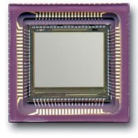
Manufacturer Part Number
CYII5SC1300-EVAL
Description
BOARD EVAL IMG SENS IBIS5-B-1300
Manufacturer
Cypress Semiconductor Corp
Specifications of CYII5SC1300-EVAL
Sensor Type
CMOS Imaging, Color (RGB)
Sensing Range
1.3 Megapixel
Interface
Parallel/Serial
Sensitivity
106 fps
Voltage - Supply
3 V ~ 4.5 V
Embedded
No
Utilized Ic / Part
IBIS5-B-1300
Lead Free Status / RoHS Status
Contains lead / RoHS non-compliant
Lead Free Status / RoHS Status
Lead free / RoHS Compliant, Contains lead / RoHS non-compliant


Document #: 38-05710 Rev. *A
Table 10.Internal Registers (continued)
Detailed Description of the Internal Registers
Sequencer Register (7:0)
Note
1. Shutter Type (bit 0).
2. Output Amplifier Calibration (bits 1 and 2).
3. Continuous Charge (bit 3).
4. Internal Clock Granularities (bits 4, 5, 6 and 7).
2. Using a SYS_CLOCK of 40 MHz (25 ns period).
10 (1010)
11 (1011)
12 (1100)
13 (1101)
14 (1110)
15 (1111)
9 (1001)
The IBIS5-B-1300 image sensor has 2 shutter types:
0 = synchronous shutter.
1 = rolling shutter.
Bits FRAME_CAL_MODE and LINE_CAL_MODE define
the calibration mode of the output amplifier.
During every row-blanking period, a calibration is done of
the output amplifier. There are 2 calibration modes. The
FAST mode (= 0) can force a calibration in one cycle but is
not so accurate and suffers from KTC noise, while the
SLOW mode (= 1) can only make incremental adjustments
and is noise free.
Approximately 200 or more “slow” calibrations have the
same effect as 1 “fast” calibration.
Different calibration modes can be set at the beginning of
the frame (FRAME_CAL_MODE bit) and for every subse-
quent line that is read (LINE_CAL_MODE bit). The begin-
ning of a frame is defined by the Y_START input (see low-
er), Y_CLOCK defines the beginning of a new row.
For some applications it might be necessary to use contin-
uous charging of the pixel columns instead of a pre-charge
on every line sample operation.
Setting bit CONT_CHARGE to “1” activates this function.
The resistor connected to pin PC_CMD is used to control
the current level on every pixel column.
The system clock is divided several times on-chip.
The X-shift-register that controls the column/pixel readout,
is clocked by half the system clock rate. Odd and even pixel
Register
Bit
6:0
6:0
2:0
0
1
2
DACRAW_REG
DACFINE_REG
ADC register
TRISTATE_OUT
GAMMA
BIT_INV
Reserved.
Reserved.
Reserved.
Reserved.
Name
Amplifier DAC raw offset.’
Default value <6:0>: “1000000”
Amplifier DAC fine offset.
Default value <6:0>: “1000000”
Default value <2:0>: “011”
0 = Output bus in tri-state.
0 = Gamma-correction on.
1 = Bit inversion on output bus.
Table 11.SS Sequencer Clock Granularities
Table 12.X Sequencer Clock Granularities
GRAN_SS_SEQ_MSB/
GRAN_X_SEQ_MSB/
columns are switched to 2 separate buses. In the output
amplifier the pixel signals on the 2 buses are combined into
one pixel stream at the same frequency as SYS_CLOCK.
The clock, that drives the “snapshot” or synchronous shut-
ter sequencer, can be programmed using the bits
GRAN_SS_SEQ_MSB (bit 7) and GRAN_SS_SEQ_LSB
(bit 6).
This way the integration time in synchronous shutter mode
can be a multiple of 32, 64, 128 or 256 times the system
clock period. To overcome global reset issues it is advised
that the longest SS granularity is used (bits 6 and 7 set to
'1').
The clock that drives the X-sequencer can be a multiple of
4, 8, 16, or 32 times the system clock. Clocking the X-se-
quencer at a slower rate (longer row blanking time; pixel
read out speed is always equal to the SYSTEM_CLOCK)
can result in more signal swing for the same light condi-
tions.
LSB
LSB
00
01
10
11
00
01
10
11
Description
16 x SYS_CLOCK
32 x SYS_CLOCK
4 x SYS_CLOCK
8 x SYS_CLOCK
128 x SYS_CLOCK
256 x SYS_CLOCK
32 x SYS_CLOCK
64 x SYS_CLOCK
X-sequencer
SS-sequencer
Clock
CYII5FM1300AB
Clock
IBIS5-B-1300
Row Blanking
Page 13 of 42
Time Step
Integration
Time
3.5 µ s
14 µ s
28 µ s
7 µ s
800 ns
1.6 µ s
3.2 µ s
6.4 µ s
[
2
]
[
2
[+] Feedback
]
Related parts for CYII5SC1300-EVAL
Image
Part Number
Description
Manufacturer
Datasheet
Request
R

Part Number:
Description:
Manufacturer:
Cypress Semiconductor Corp
Datasheet:
Part Number:
Description:
Manufacturer:
Cypress Semiconductor Corp
Datasheet:
Part Number:
Description:
Manufacturer:
Cypress Semiconductor Corp
Datasheet:
Part Number:
Description:
Manufacturer:
Cypress Semiconductor Corp
Datasheet:
Part Number:
Description:
Manufacturer:
Cypress Semiconductor Corp
Datasheet: