CYII5SC1300-EVAL Cypress Semiconductor Corp, CYII5SC1300-EVAL Datasheet - Page 7
CYII5SC1300-EVAL
Manufacturer Part Number
CYII5SC1300-EVAL
Description
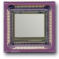
BOARD EVAL IMG SENS IBIS5-B-1300
Manufacturer
Cypress Semiconductor Corp
Specifications of CYII5SC1300-EVAL
Sensor Type
CMOS Imaging, Color (RGB)
Sensing Range
1.3 Megapixel
Interface
Parallel/Serial
Sensitivity
106 fps
Voltage - Supply
3 V ~ 4.5 V
Embedded
No
Utilized Ic / Part
IBIS5-B-1300
Lead Free Status / RoHS Status
Contains lead / RoHS non-compliant
Lead Free Status / RoHS Status
Lead free / RoHS Compliant, Contains lead / RoHS non-compliant


Document #: 38-05710 Rev. *A
Table 7. Y–Sub-sample Patterns
In normal mode the pointer for the pixel row is shifted one at
the time.
When sub-sampling is enabled, Y_SYNC is activated. The
Y-shift register shifts 2 succeeding bits and skips the 2 next
bits. This results in pattern “XXOOXXOO”.
Activating Y_SWAP12 results in pattern “XOXOXOXO”.
Activating Y_SWAP30 results in pattern “OXOXOXOX”.
Activating both Y_SWAP12 and Y_SWAP30 results in pattern
“OOXXOOXX”.
The addressable pixels range when Y-sub sampling is enabled
is: 0–1, 4–5, 8–9, 12–13, … 1020–1021
Output Amplifier
Architecture and Settings
The output amplifier stage is user-programmable for gain and
offset level. Gain is controlled by 4-bit wide word; offset by a
7-bit wide word. Gain settings are on an exponential scale.
Offset is controlled by a 7-bit wide DAC, which selects the
offset voltage between 2 reference voltages (DAC_VHIGH
and DAC_VLOW) on a linear scale.
The amplifier is designed to match the specifications of the
output of the imager array. This signal has a data rate of
40 MHz and is located between 1.17V and 2.95V. The output
impedance of the amplifier is 260 Ω .
The output signal has a range between 1.17V and 2.95V,
depending on the gain and offset settings of the amplifier. At
unity gain and with a mid-range offset value, the amplifier
outputs a signal in between 1.59V (light) and 2.70V (dark).
This analog range should fit to the input range of the ADC,
external or internal. The output swing in unity gain is approxi-
mately 1.11V and maximum 1.78V at the highest gain settings.
Figure 8 on page 8
amplifier. The odd and even column amplifiers sample both
pixel and reset value to perform a double sampling FPN
1
1
0
1
DEC(n+1)
DEC(n+2)
DEC(n+3)
DEC(n+4)
shows the architecture of the output
Y_SYNC Y_SUB
1
1
OXOXOXOX
OOXXOOXX
Reg(n+1)
Reg(n+2)
Reg(n+3)
Reg(n+4)
Reg(n)
Figure 7. Row Structure
Y_SWAP12
-correction. There are 2 different offsets that can be adjusted
using the on-chip DAC (7 bit): DAC_FINE and DAC_RAW.
DAC_FINE is used to tune the difference between odd and
even columns; DAC_RAW is used to add a general (both even
and odd columns) to the FPN corrected pixel value. This pixel
value is fed to the first amplifier stage which has an adjustable
gain, controlled by a 4-bit word (“GAIN [0…3]”).
After this, a unity feedback amplifier buffers the signal and the
signal leaves the chip. This 2nd amplifier stage determines the
maximal readout speed, that is, the bandwidth and the slew
rate of the output signal. The whole amplifier chain is designed
for a data rate of 40 Mpix/s (@20 pF).
Output Amplifier Gain Control
The output amplifier gain is controlled by a 4-bit word set in the
AMPLIFIER register (see section
page
Table 8. Overview Gain Settings
Setting of the DAC Reference Voltage
In the output amplifier, the offset can be trimmed by loading
registers DACRAW_REG and DACFINE_REG. DAC_RAW is
used to adjust the offset of the output amplifier and DAC_FINE
is used to tune the offset between the even and odd columns.
These registers are inputs for 2 DACs (see
8) that operate on the same resistor that is connected between
pins DAC_VHIGH and DAC_VLOW. The range of the DAC is
defined using a resistive division with R
R
VLOW
Y_SWAP30
15). An overview of the gain settings is given in
.
0000
0001
0010
0100
0101
0011
0110
0111
bits
SRH
SRH
SRH
SRH
DC Gain
1.37
1.62
1.96
2.33
2.76
3.50
4.25
5.20
ROW(n+1)
ROW(n+2)
ROW(n+3)
ROW(n+4)
CYII5FM1300AB
“Amplifier Register (6:0)” on
IBIS5-B-1300
1000
1001
1010
1011
1100
1101
1110
1111
bits
VHIGH
Figure 9 on page
Page 7 of 42
, R
DC Gain
11.00
11.37
11.84
12.32
12.42
6.25
7.89
9.21
DAC
Table
and
8.
[+] Feedback
Related parts for CYII5SC1300-EVAL
Image
Part Number
Description
Manufacturer
Datasheet
Request
R

Part Number:
Description:
Manufacturer:
Cypress Semiconductor Corp
Datasheet:
Part Number:
Description:
Manufacturer:
Cypress Semiconductor Corp
Datasheet:
Part Number:
Description:
Manufacturer:
Cypress Semiconductor Corp
Datasheet:
Part Number:
Description:
Manufacturer:
Cypress Semiconductor Corp
Datasheet:
Part Number:
Description:
Manufacturer:
Cypress Semiconductor Corp
Datasheet: