CYII5SC1300-EVAL Cypress Semiconductor Corp, CYII5SC1300-EVAL Datasheet - Page 22
CYII5SC1300-EVAL
Manufacturer Part Number
CYII5SC1300-EVAL
Description
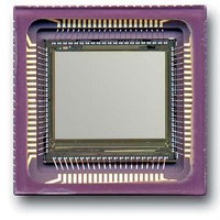
BOARD EVAL IMG SENS IBIS5-B-1300
Manufacturer
Cypress Semiconductor Corp
Specifications of CYII5SC1300-EVAL
Sensor Type
CMOS Imaging, Color (RGB)
Sensing Range
1.3 Megapixel
Interface
Parallel/Serial
Sensitivity
106 fps
Voltage - Supply
3 V ~ 4.5 V
Embedded
No
Utilized Ic / Part
IBIS5-B-1300
Lead Free Status / RoHS Status
Contains lead / RoHS non-compliant
Lead Free Status / RoHS Status
Lead free / RoHS Compliant, Contains lead / RoHS non-compliant


Document #: 38-05710 Rev. *A
Pin List
The IBIS5-B-1300 image sensor is packaged in a leadless ceramic carrier (LCC package).
their functions. In total, there are 84 pins.
Table 20.Pin List
Notes
3. All pins with the same name can be connected together.
4. All digital input are active high (unless mentioned otherwise).
5. Digital inputs that are not used must be tied to GND (inactive level).
Pin
10
12
13
14
15
16
17
18
19
20
21
22
23
24
25
26
27
28
29
30
11
1
2
3
4
5
6
7
8
9
P_DATA<8>
P_WR
S_CLK
S_DATA
S_EN
SER_MODE
VDDC
VDDA
GNDA
GNDD
VDDD
IF_MODE
DEC_CMD
Y_START
Y_CLOCK
LAST_LINE
X_LOAD
SYS_CLOCK
PXL_VALID
SS_START
SS_STOP
TIME_OUT
SYS_RESET
EL_BLACK
EOSX
DAC_VHIGH
DAC_VLOW
PXL_OUT1
PXL_OUT2
AMP_CMD
Pin Name
[
3
,
4
,
5
]
Input
Input
Input
Input
Input
Input
Supply
Supply
Ground
Ground
Supply
Input
Input
Input
Input
Output
Input
Input
Output
Input
Input
Output
Input
Input
Output
Input
Input
Output
Output
Input
Pin Type
Digital input. Data parallel interface.
Digital input (active high). Parallel write.
Digital input. Clock signal of serial interface.
Digital input/output. Data of serial interface.
Digital input (active low). Enable of Serial-3-wire interface.
Digital input. Serial mode enable (1 = Enable serial-3-wire, 0 = Enable serial-2-wire).
Analog supply voltage. Supply voltage of the pixel core [3.3V].
Analog supply voltage. Analog supply voltage of the image sensor [3.3V].
Analog ground. Analog ground of the image sensor.
Digital ground. Digital ground of the image sensor.
Digital supply voltage. Digital supply voltage of the image sensor [3.3V].
Digital input. Interface mode (1 = parallel; 0 = serial).
Analog input. Biasing of decoder stage. Connect to VDDA with R = 50 k Ω and decouple
with C = 100 nF to GNDA.
Digital input (active high). Start frame read out.
Digital input (active high). Line clock.
Digital output. Generates a high level when the last line is read out.
Digital input (active high). Loads new X-position during read out.
Digital input. System (pixel) clock (40 MHz).
Digital output. Generates high level during pixel read out.
Digital input (active high). Start synchronous shutter operation.
Digital input (active high). Stop synchronous shutter operation.
Digital output.
Synchronous shutter: pulse when time-out reached. Can be used to trigger SS_STOP
although both signals can't be tied together.
Rolling shutter: pulse when second Y-sync appears.
Digital input (active high). Global system reset.
Digital input (active high). Enables electrical black in output amplifier.
Digital output. Diagnostic end-of-scan of X-register.
Analog reference input. Biasing of DAC for output dark level. Can be used to set output
range of DAC.
Default: Connect to VDDA with R = 0 Ω .
Analog reference input. Biasing of DAC for output dark level. Can be used to set output
range of DAC.
Default: Connect to GND A with R = 0 Ω .
Analog output. Analog pixel output 1.
Analog output. Analog pixel output 2. Leave not connected if not used.
Analog input. Biasing of the output amplifier. Connect to VDDA with R = 50 k Ω and
decouple with C = 100 nF to GNDA.
Pin Description
Table 20
CYII5FM1300AB
is a list of all the pins and
IBIS5-B-1300
Page 22 of 42
[+] Feedback
Related parts for CYII5SC1300-EVAL
Image
Part Number
Description
Manufacturer
Datasheet
Request
R

Part Number:
Description:
Manufacturer:
Cypress Semiconductor Corp
Datasheet:
Part Number:
Description:
Manufacturer:
Cypress Semiconductor Corp
Datasheet:
Part Number:
Description:
Manufacturer:
Cypress Semiconductor Corp
Datasheet:
Part Number:
Description:
Manufacturer:
Cypress Semiconductor Corp
Datasheet:
Part Number:
Description:
Manufacturer:
Cypress Semiconductor Corp
Datasheet: