DK-DEV-3SL150N Altera, DK-DEV-3SL150N Datasheet - Page 11
DK-DEV-3SL150N
Manufacturer Part Number
DK-DEV-3SL150N
Description
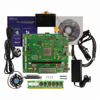
KIT DEVELOPMENT STRATIX III
Manufacturer
Altera
Series
Stratix® IIIr
Type
FPGAr
Datasheets
1.EP3SL150F780C4N.pdf
(16 pages)
2.EP3SL150F780C4N.pdf
(332 pages)
3.DK-DEV-3SL150N.pdf
(34 pages)
Specifications of DK-DEV-3SL150N
Contents
Development Platform, Cables and Software
Silicon Manufacturer
Altera
Core Architecture
FPGA
Core Sub-architecture
Stratix
Silicon Core Number
EP3S
Silicon Family Name
Stratix III
Kit Contents
Development Board, Cable And Accessories
Rohs Compliant
Yes
For Use With/related Products
EP3SL150F152
Lead Free Status / RoHS Status
Lead free / RoHS Compliant
Other names
544-2568
Available stocks
Company
Part Number
Manufacturer
Quantity
Price
Company:

Part Number:
DK-DEV-3SL150N
Manufacturer:
Altera
Quantity:
135


Chapter 1: Stratix III Device Family Overview
Architecture Features
Remote System Upgrades
IEEE 1149.1 (JTAG) Boundary-Scan Testing
Design Security
© March 2010 Altera Corporation
f
f
f
Stratix III devices support configuration data decompression, which saves
configuration memory space and time. This feature allows you to store compressed
configuration data in configuration devices or other memory and transmit this
compressed bitstream to Stratix III devices. During configuration, the Stratix III
device decompresses the bitstream in real time and programs its SRAM cells.
Stratix III devices support decompression in the FPP when using a MAX II
device/microprocessor plus flash, fast AS, and PS configuration schemes. The
Stratix III decompression feature is not available in the FPP when using the enhanced
configuration device and JTAG configuration schemes.
For more information, refer to the
Stratix III devices feature remote system upgrade capability, allowing error-free
deployment of system upgrades from a remote location securely and reliably. Soft
logic (either the Nios embedded processor or user logic) implemented in a Stratix III
device can download a new configuration image from a remote location, store it in
configuration memory, and direct the dedicated remote system upgrade circuitry to
initiate a reconfiguration cycle. The dedicated circuitry performs error detection
during and after the configuration process, and can recover from an error condition
by reverting back to a safe configuration image, and provides error status
information. This dedicated remote system upgrade circuitry is unique to Stratix
series FPGAs and helps to avoid system downtime.
For more information, refer to the
chapter.
Stratix III devices support the JTAG IEEE Std. 1149.1 specification. The Boundary-Scan
Test (BST) architecture offers the capability to test pin connections without using
physical test probes and capture functional data while a device is operating normally.
Boundary-scan cells in the Stratix III device can force signals onto pins or capture data
from pin or logic array signals. Forced test data is serially shifted into the
boundary-scan cells. Captured data is serially shifted out and externally compared to
expected results. In addition to BST, you can use the IEEE Std. 1149.1 controller for
Stratix III device in-circuit reconfiguration (ICR).
For more information, refer to the
Stratix III Devices
Stratix III devices are high-density, high-performance FPGAs with support for 256-bit
volatile and non-volatile security keys to protect designs against copying, reverse
engineering, and tampering. Stratix III devices have the ability to decrypt a
configuration bitstream using the Advanced Encryption Standard (AES) algorithm,
an industry standard encryption algorithm that is FIPS-197 certified and requires a
256-bit security key.
chapter.
Configuring Stratix III Devices
Remote System Upgrades with Stratix III Devices
IEEE 1149.1 (JTAG) Boundary Scan Testing in
Stratix III Device Handbook, Volume 1
chapter.
1–11
Related parts for DK-DEV-3SL150N
Image
Part Number
Description
Manufacturer
Datasheet
Request
R

Part Number:
Description:
KIT DEV ARRIA II GX FPGA 2AGX125
Manufacturer:
Altera
Datasheet:

Part Number:
Description:
KIT DEV CYCLONE III LS EP3CLS200
Manufacturer:
Altera
Datasheet:

Part Number:
Description:
KIT DEV STRATIX IV FPGA 4SE530
Manufacturer:
Altera
Datasheet:

Part Number:
Description:
KIT DEV FPGA 2AGX260 W/6.375G TX
Manufacturer:
Altera
Datasheet:

Part Number:
Description:
KIT DEV MAX V 5M570Z
Manufacturer:
Altera
Datasheet:

Part Number:
Description:
KIT DEV STRATIX V FPGA 5SGXEA7
Manufacturer:
Altera
Datasheet:

Part Number:
Description:
KIT DEVELOPMENT STRATIX IV
Manufacturer:
Altera
Datasheet:

Part Number:
Description:
KIT DEV ARRIA GX 1AGX60N
Manufacturer:
Altera
Datasheet:
Part Number:
Description:
KIT STARTER CYCLONE IV GX
Manufacturer:
Altera
Datasheet:
Part Number:
Description:
KIT DEVELOPMENT STRATIX IV
Manufacturer:
Altera
Datasheet:

Part Number:
Description:
CPLD, EP610 Family, ECMOS Process, 300 Gates, 16 Macro Cells, 16 Reg., 16 User I/Os, 5V Supply, 35 Speed Grade, 24DIP
Manufacturer:
Altera Corporation
Datasheet:
Part Number:
Description:
CPLD, EP610 Family, ECMOS Process, 300 Gates, 16 Macro Cells, 16 Reg., 16 User I/Os, 5V Supply, 15 Speed Grade, 24DIP
Manufacturer:
Altera Corporation
Datasheet: