HW-SD1800A-DSP-SB-UNI-G Xilinx Inc, HW-SD1800A-DSP-SB-UNI-G Datasheet - Page 11
HW-SD1800A-DSP-SB-UNI-G
Manufacturer Part Number
HW-SD1800A-DSP-SB-UNI-G
Description
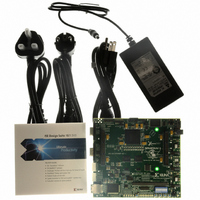
KIT DEVELOPMENT SPARTAN 3ADSP
Manufacturer
Xilinx Inc
Series
Spartan™-3A DSPr
Type
DSPr
Datasheet
1.HW-SD1800A-DSP-SB-UNI-G.pdf
(38 pages)
Specifications of HW-SD1800A-DSP-SB-UNI-G
Contents
Development Platform, Power Supply and software
Silicon Manufacturer
Xilinx
Features
10/100/1000 PHY, JTAG Programming And Configuration Port
Silicon Family Name
Spartan-3A
Silicon Core Number
3SD1800A-FG676
Lead Free Status / RoHS Status
Lead free / RoHS Compliant
For Use With/related Products
Spartan 3A
Lead Free Status / RoHS Status
Lead free / RoHS Compliant, Lead free / RoHS Compliant
Other names
122-1574
HW-SD1800A-DSP-DB-UNI-G
HW-SD1800A-DSP-DB-UNI-G
HW-SD1800A-DSP-SB-UNI-G
HW-SD1800A-DSP-DB-UNI-G
HW-SD1800A-DSP-DB-UNI-G
HW-SD1800A-DSP-SB-UNI-G
Available stocks
Company
Part Number
Manufacturer
Quantity
Price


Spartan-3A DSP Starter Platform User Guide
UG454 (v1.1) January 30, 2009
R
•
•
•
All DDR2 routing is length-matched within certain tolerances; these are:
•
•
•
•
The DDR2 signals are connected to I/O Bank 3 of the Spartan-3 SA DSP FPGA. The output
supply pins (VCCO) for Bank 3 is connected to 1.8 Volts. A Texas Instruments TPS51116
Buck Controller and ancillary circuitry provides the 1.8V DDR2 power, the 0.9V
termination voltage (FPGA_0.9V_TT) and the DDR2 reference voltage
(FPGA_DDR2_VREF). This power source also supplies the 1.8V core voltage to the
Ethernet PHY.
Table 3: FPGA DDR2 Interface Pinout
60-ohm pull-up resistor to the termination supply at the split-point of shared signals
(control, address)
Termination supply that can both source and sink current
Feedback clock routed with twice the length to simulate the total flight time
Members of a differential pair matched to +/-10mil
DQ, DQS, DM and CK matched to +/- 45mil
Control matched to +/- 100mil of data interface
RST_DQS_DIV and MB_FB_CLK matched to +/- 45mil of sum of average DQS and
average CK
FPGA_DDR_CAS#
FPGA_DDR_RAS#
FPGA_DDR_WE#
FPGA_DDR_CKE
FPGA_DDR_A10
FPGA_DDR_A11
FPGA_DDR_A12
FPGA_DDR_CS#
FPGA_DDR_BS0
FPGA_DDR_BS1
FPGA_DDR_A0
FPGA_DDR_A1
FPGA_DDR_A2
FPGA_DDR_A3
FPGA_DDR_A4
FPGA_DDR_A5
FPGA_DDR_A6
FPGA_DDR_A7
FPGA_DDR_A8
FPGA_DDR_A9
DDR2 Signal
www.xilinx.com
FPGA Pin
Number
M10
L10
M8
M7
M8
M3
M4
H1
H2
K4
K5
K2
K3
K6
L3
L4
L9
L7
J5
J4
FPGA_DDR_UDM_1
FPGA_DDR_LDM_0
FPGA_DDR_LDM_0
FPGA_DDR_LDM_1
DDR2_ODT_Control
FPGA_DDR_D10
FPGA_DDR_D12
FPGA_DDR_D13
FPGA_DDR_D14
FPGA_DDR_D11
FPGA_DDR_D0
FPGA_DDR_D1
FPGA_DDR_D2
FPGA_DDR_D3
FPGA_DDR_D4
FPGA_DDR_D5
FPGA_DDR_D6
FPGA_DDR_D7
FPGA_DDR_D8
FPGA_DDR_D9
DDR2 Signal
Functional Description
FPGA Pin Number
AA2
AA3
AC1
AB1
M6
U9
U7
U8
U6
U5
V2
V1
R2
G3
V8
Y5
Y6
Y1
Y2
T7
35
Related parts for HW-SD1800A-DSP-SB-UNI-G
Image
Part Number
Description
Manufacturer
Datasheet
Request
R

Part Number:
Description:
KIT DEVELOPMENT SPARTAN 3ADSP
Manufacturer:
Xilinx Inc

Part Number:
Description:
IC CPLD .8K 36MCELL 44-VQFP
Manufacturer:
Xilinx Inc
Datasheet:

Part Number:
Description:
IC CPLD 72MCRCELL 10NS 44VQFP
Manufacturer:
Xilinx Inc
Datasheet:

Part Number:
Description:
IC CPLD 1.6K 72MCELL 64-VQFP
Manufacturer:
Xilinx Inc
Datasheet:

Part Number:
Description:
IC CR-II CPLD 64MCELL 44-VQFP
Manufacturer:
Xilinx Inc
Datasheet:

Part Number:
Description:
IC CPLD 1.6K 72MCELL 100-TQFP
Manufacturer:
Xilinx Inc
Datasheet:

Part Number:
Description:
IC CR-II CPLD 64MCELL 56-BGA
Manufacturer:
Xilinx Inc
Datasheet:

Part Number:
Description:
IC CPLD 72MCRCELL 7.5NS 44VQFP
Manufacturer:
Xilinx Inc
Datasheet:
Part Number:
Description:
IC CR-II CPLD 64MCELL 100-VQFP
Manufacturer:
Xilinx Inc
Datasheet:
Part Number:
Description:
IC CPLD 1.6K 72MCELL 100-TQFP
Manufacturer:
Xilinx Inc
Datasheet:

Part Number:
Description:
IC CPLD 72MCRCELL 7.5NS 64VQFP
Manufacturer:
Xilinx Inc
Datasheet:
Part Number:
Description:
IC CPLD 1.6K 72MCELL 100-TQFP
Manufacturer:
Xilinx Inc
Datasheet:

Part Number:
Description:
IC CPLD 1.5K 64MCELL HP 44-VQFP
Manufacturer:
Xilinx Inc

Part Number:
Description:
IC CPLD 36MCRCELL 15NS 44PLCC
Manufacturer:
Xilinx Inc
Datasheet:

Part Number:
Description:
IC CPLD 36MCRCELL 10NS 44PLCC
Manufacturer:
Xilinx Inc
Datasheet: