HW-SD1800A-DSP-SB-UNI-G Xilinx Inc, HW-SD1800A-DSP-SB-UNI-G Datasheet - Page 23
HW-SD1800A-DSP-SB-UNI-G
Manufacturer Part Number
HW-SD1800A-DSP-SB-UNI-G
Description
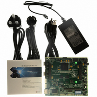
KIT DEVELOPMENT SPARTAN 3ADSP
Manufacturer
Xilinx Inc
Series
Spartan™-3A DSPr
Type
DSPr
Datasheet
1.HW-SD1800A-DSP-SB-UNI-G.pdf
(38 pages)
Specifications of HW-SD1800A-DSP-SB-UNI-G
Contents
Development Platform, Power Supply and software
Silicon Manufacturer
Xilinx
Features
10/100/1000 PHY, JTAG Programming And Configuration Port
Silicon Family Name
Spartan-3A
Silicon Core Number
3SD1800A-FG676
Lead Free Status / RoHS Status
Lead free / RoHS Compliant
For Use With/related Products
Spartan 3A
Lead Free Status / RoHS Status
Lead free / RoHS Compliant, Lead free / RoHS Compliant
Other names
122-1574
HW-SD1800A-DSP-DB-UNI-G
HW-SD1800A-DSP-DB-UNI-G
HW-SD1800A-DSP-SB-UNI-G
HW-SD1800A-DSP-DB-UNI-G
HW-SD1800A-DSP-DB-UNI-G
HW-SD1800A-DSP-SB-UNI-G
Available stocks
Company
Part Number
Manufacturer
Quantity
Price


Spartan-3A DSP Starter Platform User Guide
UG454 (v1.1) January 30, 2009
R
Expansion Connectors
EXP Interfaces
The Spartan-3A DSP Starter Platform provides expansion capabilities for customized user
application daughter cards and interfaces over two EXP expansion connectors. The EXP
expansion connectors on the board can support two half-card EXP modules or a single
dual slot EXP module. Both off-the-shelf EXP modules and user-developed modules can
easily be plugged onto the Spartan-3A DSP Starter Platform to add features and functions
to the backend application of the main board.
The EXP specification defines a 132-pin connector, with 24 power I/Os, 24 grounds I/Os,
and 84 user I/Os. The standard EXP configuration implemented on the Spartan-3A DSP
Starter Platform uses two connectors (Samtec part number QTE-060-09-F-D-A) in a dual
slot EXP configuration, for a total of 168 user I/Os. Using a jumper, the voltage levels for
the EXP user I/O can be set to either 2.5V or 3.3V. As shown in
the I/O voltage for the EXP connectors labeled JX1 and JX2 respectively, by setting the
VCCO voltage for the banks of the FPGA that connect to the EXP I/O.
an overview of the EXP signals; Tables 17 and 18 provide the FPGA pinouts for EXP con-
nectors JX1 and JX2, respectively.
blades (numbered 122 through 131 on the schematic and PCB) that are positioned in the
center of the connector. Technically, these are not pins and are not identified as such in this
document. For more information on the EXP open specification from Avnet, see
www.em.avnet.com/exp.
X-Ref Target - Figure 8
The EXP specification defines four user signal types:
Single Ended I/O, Differential I/O, Differential, Single Ended Clock Inputs, and
Differential and Single Ended Clock Outputs. Because the FPGA I/Os can be configured
for either single-ended or differential use, the differential I/Os defined in the EXP
Connector
EXP
JX1
2.5V
3.3V
JX1_VCCO
User IO
JP2
www.xilinx.com
VCCO_0
Figure 8: EXP I/O Voltage Settings
Bank 0
Vcco
Table 16
3A DSP
Spartan
and
Table 17
Bank 2
Bank 1
(8 IOs)
Vcco
+
VCCO_2
do not show the connector ground
JX2_VCCO
JP2
User IO
Figure
Functional Description
3.3V
2.5V
8, JP2 and JP3 set
Table 15
Connector
UG454_08_050908
EXP
JX2
provides
47
Related parts for HW-SD1800A-DSP-SB-UNI-G
Image
Part Number
Description
Manufacturer
Datasheet
Request
R

Part Number:
Description:
KIT DEVELOPMENT SPARTAN 3ADSP
Manufacturer:
Xilinx Inc

Part Number:
Description:
IC CPLD .8K 36MCELL 44-VQFP
Manufacturer:
Xilinx Inc
Datasheet:

Part Number:
Description:
IC CPLD 72MCRCELL 10NS 44VQFP
Manufacturer:
Xilinx Inc
Datasheet:

Part Number:
Description:
IC CPLD 1.6K 72MCELL 64-VQFP
Manufacturer:
Xilinx Inc
Datasheet:

Part Number:
Description:
IC CR-II CPLD 64MCELL 44-VQFP
Manufacturer:
Xilinx Inc
Datasheet:

Part Number:
Description:
IC CPLD 1.6K 72MCELL 100-TQFP
Manufacturer:
Xilinx Inc
Datasheet:

Part Number:
Description:
IC CR-II CPLD 64MCELL 56-BGA
Manufacturer:
Xilinx Inc
Datasheet:

Part Number:
Description:
IC CPLD 72MCRCELL 7.5NS 44VQFP
Manufacturer:
Xilinx Inc
Datasheet:
Part Number:
Description:
IC CR-II CPLD 64MCELL 100-VQFP
Manufacturer:
Xilinx Inc
Datasheet:
Part Number:
Description:
IC CPLD 1.6K 72MCELL 100-TQFP
Manufacturer:
Xilinx Inc
Datasheet:

Part Number:
Description:
IC CPLD 72MCRCELL 7.5NS 64VQFP
Manufacturer:
Xilinx Inc
Datasheet:
Part Number:
Description:
IC CPLD 1.6K 72MCELL 100-TQFP
Manufacturer:
Xilinx Inc
Datasheet:

Part Number:
Description:
IC CPLD 1.5K 64MCELL HP 44-VQFP
Manufacturer:
Xilinx Inc

Part Number:
Description:
IC CPLD 36MCRCELL 15NS 44PLCC
Manufacturer:
Xilinx Inc
Datasheet:

Part Number:
Description:
IC CPLD 36MCRCELL 10NS 44PLCC
Manufacturer:
Xilinx Inc
Datasheet: