ADZS-BF518F-EZBRD Analog Devices Inc, ADZS-BF518F-EZBRD Datasheet - Page 11
ADZS-BF518F-EZBRD
Manufacturer Part Number
ADZS-BF518F-EZBRD
Description
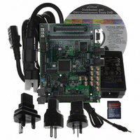
BOARD EVAL BF512F/14F/16F/18F
Manufacturer
Analog Devices Inc
Series
Blackfin®r
Type
DSPr
Specifications of ADZS-BF518F-EZBRD
Featured Product
Blackfin® BF50x Series Processors
Contents
Board, Cables, CD
Silicon Manufacturer
Analog Devices
Core Architecture
Blackfin
Features
JTAG Emulator Or Standalone Debug Agent Board
Kit Contents
Board Only
Silicon Family Name
Blackfin
Architecture
DSP
Ide Included
Visual DSP++
Code Gen Tools Included
Visual DSP++
Debugger Included
Visual DSP++
Silicon Core Number
ADSP-BF518F
Rohs Compliant
Yes
Lead Free Status / RoHS Status
Lead free / RoHS Compliant
For Use With/related Products
BF512F/14F/16F/18F
For Use With
ADZS-BFBLUET-EZEXT - EZ-EXTENDER DAUGHTERBOARD
Lead Free Status / Rohs Status
Supplier Unconfirmed


Preliminary Technical Data
mode. In single update mode the duty cycle values are program-
mable only once per PWM period, so that the resultant PWM
patterns are symmetrical about the midpoint of the PWM
period. In the double update mode, a second updating of the
PWM registers is implemented at the midpoint of the PWM
period. In this mode, it is possible to produce asymmetrical
PWM patterns that produce lower harmonic distortion in
3-phase PWM inverters.
GENERAL-PURPOSE (GP) COUNTER
A 32-bit GP counter is provided that can sense 2-bit quadrature
or binary codes as typically emitted by industrial drives or man-
ual thumb wheels. The counter can also operate in general-
purpose up/down count modes. Then, count direction is either
controlled by a level-sensitive input signal or by two edge
detectors.
A third input can provide flexible zero marker support and can
alternatively be used to input the push-button signal of thumb
wheels. All three signals have a programmable debouncing
circuit.
An internal signal forwarded to the GP timer unit enables one
timer to measure the intervals between count events. Boundary
registers enable auto-zero operation or simple system warning
by interrupts when programmable count values are exceeded.
SERIAL PORTS
The ADSP-BF512/BF514/BF516/BF518(F) processors incorpo-
rate two dual-channel synchronous serial ports (SPORT0 and
SPORT1) for serial and multiprocessor communications. The
SPORTs support the following features:
• I
• Bidirectional operation – Each SPORT has two sets of inde-
• Buffered (8-deep) transmit and receive ports – Each port
• Clocking – Each transmit and receive port can either use an
• Word length – Each SPORT supports serial data words
• Framing – Each transmit and receive port can run with or
• Companding in hardware – Each SPORT can perform
pendent transmit and receive signals, enabling eight
channels of I
has a data register for transferring data words to and from
other processor components and shift registers for shifting
data in and out of the data registers.
external serial clock or generate its own, in frequencies
ranging from (f
from 3 to 32 bits in length, transferred most-significant-bit
first or least-significant-bit first.
without frame sync signals for each data word. Frame sync
signals can be generated internally or externally, active high
or low, and with either of two pulse widths and early or late
frame sync.
A-law or μ-law companding according to ITU recommen-
dation G.711. Companding can be selected on the transmit
and/or receive channel of the SPORT without
additional latencies.
2
S capable operation.
2
S stereo audio.
SCLK
/131,070) Hz to (f
SCLK
/2) Hz.
Rev. PrE | Page 11 of 62 | March 2009
SERIAL PERIPHERAL INTERFACE (SPI) PORTS
The processors have two SPI-compatible ports (SPI0 and SPI1)
that enable the processor to communicate with multiple SPI-
compatible devices.
The SPI interface uses three signals for transferring data: two
data signals (master output-slave input–MOSI, and master
input-slave output–MISO) and a clock signal (serial
clock–SCK). An SPI chip select input signal (SPIxSS) lets other
SPI devices select the processor, and multiple SPI chip select
output signals let the processor select other SPI devices. The SPI
select signals are reconfigured general-purpose I/O signals.
Using these signals, the SPI port provides a full-duplex, syn-
chronous serial interface, which supports both master/slave
modes and multimaster environments.
The SPI port baud rate and clock phase/polarities are program-
mable, and it has an integrated DMA channel, configurable to
support transmit or receive data streams. The SPI’s DMA chan-
nel can only service unidirectional accesses at any given time.
The SPI port clock rate is calculated as:
Where the 16-bit SPI_BAUD register contains a value of 2
to 65,535.
During transfers, the SPI port simultaneously transmits and
receives by serially shifting data in and out on its two serial data
lines. The serial clock line synchronizes the shifting and sam-
pling of data on the two serial data lines.
UART PORTS
The ADSP-BF512/BF514/BF516/BF518(F) processors provide
two full-duplex universal asynchronous receiver/transmitter
(UART) ports, which are fully compatible with PC-standard
UARTs. Each UART port provides a simplified UART interface
to other peripherals or hosts, supporting full-duplex, DMA-sup-
ported, asynchronous transfers of serial data. A UART port
ADSP-BF512/BF514/BF516/BF518(F)
• DMA operations with single-cycle overhead – Each SPORT
• Interrupts – Each transmit and receive port generates an
• Multichannel capability – Each SPORT supports 128 chan-
can automatically receive and transmit multiple buffers of
memory data. The processor can link or chain sequences of
DMA transfers between a SPORT and memory.
interrupt upon completing the transfer of a data word or
after transferring an entire data buffer, or buffers,
through DMA.
nels out of a 1024-channel window and is compatible with
the H.100, H.110, MVIP-90, and HMVIP standards.
SPI Clock Rate
=
----------------------------------- -
2
SPI_BAUD
f
SCLK
Related parts for ADZS-BF518F-EZBRD
Image
Part Number
Description
Manufacturer
Datasheet
Request
R

Part Number:
Description:
BLACKFIN EZ-EXTENDER Board For ADSP-BF533/61 EZ-KIT LITE
Manufacturer:
Analog Devices Inc

Part Number:
Description:
±1.7g Dual-Axis IMEMS Accelerometer Evaluation Board
Manufacturer:
Analog Devices Inc
Datasheet:

Part Number:
Description:
Inertial Sensor Evaluation System
Manufacturer:
Analog Devices Inc
Datasheet:
Part Number:
Description:
Manufacturer:
Analog Devices Inc
Datasheet:
Part Number:
Description:
Manufacturer:
Analog Devices Inc
Datasheet:
Part Number:
Description:
Manufacturer:
Analog Devices Inc
Datasheet:
Part Number:
Description:
Manufacturer:
Analog Devices Inc
Datasheet:
Part Number:
Description:
Manufacturer:
Analog Devices Inc
Datasheet:
Part Number:
Description:
Manufacturer:
Analog Devices Inc
Datasheet:
Part Number:
Description:
Manufacturer:
Analog Devices Inc
Datasheet:
Part Number:
Description:
Manufacturer:
Analog Devices Inc
Datasheet:
Part Number:
Description:
Manufacturer:
Analog Devices Inc
Datasheet:
Part Number:
Description:
Manufacturer:
Analog Devices Inc
Datasheet: