ADZS-BF518F-EZBRD Analog Devices Inc, ADZS-BF518F-EZBRD Datasheet - Page 52
ADZS-BF518F-EZBRD
Manufacturer Part Number
ADZS-BF518F-EZBRD
Description
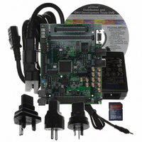
BOARD EVAL BF512F/14F/16F/18F
Manufacturer
Analog Devices Inc
Series
Blackfin®r
Type
DSPr
Specifications of ADZS-BF518F-EZBRD
Featured Product
Blackfin® BF50x Series Processors
Contents
Board, Cables, CD
Silicon Manufacturer
Analog Devices
Core Architecture
Blackfin
Features
JTAG Emulator Or Standalone Debug Agent Board
Kit Contents
Board Only
Silicon Family Name
Blackfin
Architecture
DSP
Ide Included
Visual DSP++
Code Gen Tools Included
Visual DSP++
Debugger Included
Visual DSP++
Silicon Core Number
ADSP-BF518F
Rohs Compliant
Yes
Lead Free Status / RoHS Status
Lead free / RoHS Compliant
For Use With/related Products
BF512F/14F/16F/18F
For Use With
ADZS-BFBLUET-EZEXT - EZ-EXTENDER DAUGHTERBOARD
Lead Free Status / Rohs Status
Supplier Unconfirmed


ADSP-BF512/BF514/BF516/BF518(F)
BF512/BF514/BF516/BF518(F) processor’s output voltage and
the input threshold for the device requiring the hold time. C
the total bus capacitance (per data line), and I
age or three-state current (per data line). The hold time will be
t
Timing Specifications on Page 27
SDRAM write cycle as shown in
Page
Capacitive Loading
Output delays and holds are based on standard capacitive loads:
30 pF on all pins/balls (see
(nominal) = 2.5 V/3.3 V.
Figure 55 on Page 53
capacitance. The delay and hold specifications given should be
derated by a factor derived from these figures. The graphs in
these figures may not be linear outside the ranges shown.
DECAY
V
LOAD
NOTES:
THE WORST CASE TRANSMISSION LINE DELAY IS SHOWN AND CAN BE USED
FOR THE OUTPUT TIMING ANALYSIS TO REFELECT THE TRANSMISSION LINE
EFFECT AND MUST BE CONSIDERED. THE TRANSMISSION LINE (TD), IS FOR
LOAD ONLY AND DOES NOT AFFECT THE DATA SHEET TIMING SPECIFICATIONS.
ANALOG DEVICES RECOMMENDS USING THE IBIS MODEL TIMING FOR A GIVEN
SYSTEM REQUIREMENT. IF NECESSARY, A SYSTEM MAY INCORPORATE
EXTERNAL DRIVERS TO COMPENSATE FOR ANY TIMING DIFFERENCES.
4pF
plus the various output disable times as specified in the
30).
Figure 47. Equivalent Device Loading for AC Measurements
(Includes All Fixtures)
50
70
50
400
2pF
show how output rise time varies with
Figure 48 on Page 52
45
0.5pF
Figure
TESTER PIN ELECTRONICS
SDRAM Interface Timing on
(for example t
47). V
ZO = 50 (impedance)
TD = 4.04
LOAD
T1
is 1.5 V for V
L
1.18 ns
is the total leak-
through
DSDAT
Rev. PrE | Page 52 of 62 | March 2009
for an
OUTPUT
DUT
DDEXT
L
is
Figure 48. Typical Rise and Fall Times (10%–90%) versus Load Capacitance
Figure 49. Typical Rise and Fall Times (10%–90%) versus Load Capacitance
Figure 50. Typical Rise and Fall Times (10%–90%) versus Load Capacitance
TBD
TBD
TBD
Preliminary Technical Data
for Driver A at EVDD
for Driver A at EVDD
for Driver B at EVDD
MAX
MIN
MIN
Related parts for ADZS-BF518F-EZBRD
Image
Part Number
Description
Manufacturer
Datasheet
Request
R

Part Number:
Description:
BLACKFIN EZ-EXTENDER Board For ADSP-BF533/61 EZ-KIT LITE
Manufacturer:
Analog Devices Inc

Part Number:
Description:
±1.7g Dual-Axis IMEMS Accelerometer Evaluation Board
Manufacturer:
Analog Devices Inc
Datasheet:

Part Number:
Description:
Inertial Sensor Evaluation System
Manufacturer:
Analog Devices Inc
Datasheet:
Part Number:
Description:
Manufacturer:
Analog Devices Inc
Datasheet:
Part Number:
Description:
Manufacturer:
Analog Devices Inc
Datasheet:
Part Number:
Description:
Manufacturer:
Analog Devices Inc
Datasheet:
Part Number:
Description:
Manufacturer:
Analog Devices Inc
Datasheet:
Part Number:
Description:
Manufacturer:
Analog Devices Inc
Datasheet:
Part Number:
Description:
Manufacturer:
Analog Devices Inc
Datasheet:
Part Number:
Description:
Manufacturer:
Analog Devices Inc
Datasheet:
Part Number:
Description:
Manufacturer:
Analog Devices Inc
Datasheet:
Part Number:
Description:
Manufacturer:
Analog Devices Inc
Datasheet:
Part Number:
Description:
Manufacturer:
Analog Devices Inc
Datasheet: