ADZS-BF518F-EZBRD Analog Devices Inc, ADZS-BF518F-EZBRD Datasheet - Page 23
ADZS-BF518F-EZBRD
Manufacturer Part Number
ADZS-BF518F-EZBRD
Description
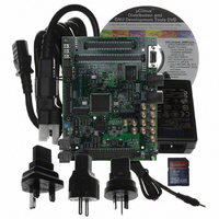
BOARD EVAL BF512F/14F/16F/18F
Manufacturer
Analog Devices Inc
Series
Blackfin®r
Type
DSPr
Specifications of ADZS-BF518F-EZBRD
Featured Product
Blackfin® BF50x Series Processors
Contents
Board, Cables, CD
Silicon Manufacturer
Analog Devices
Core Architecture
Blackfin
Features
JTAG Emulator Or Standalone Debug Agent Board
Kit Contents
Board Only
Silicon Family Name
Blackfin
Architecture
DSP
Ide Included
Visual DSP++
Code Gen Tools Included
Visual DSP++
Debugger Included
Visual DSP++
Silicon Core Number
ADSP-BF518F
Rohs Compliant
Yes
Lead Free Status / RoHS Status
Lead free / RoHS Compliant
For Use With/related Products
BF512F/14F/16F/18F
For Use With
ADZS-BFBLUET-EZEXT - EZ-EXTENDER DAUGHTERBOARD
Lead Free Status / Rohs Status
Supplier Unconfirmed


Preliminary Technical Data
SPECIFICATIONS
Note that component specifications are subject to change
without notice.
OPERATING CONDITIONS
1
2
3
4
5
6
7
8
9
10
Parameter
V
V
V
V
V
V
V
V
V
V
V
V
V
V
V
T
T
T
The expected nominal value is 1.4V 5% and initial customer designs should design with a programmable regulator that can be adjusted from 0.95V to 1.5V in 50mV steps.
Must remain powered (even if the associated function is not used).
V
If not used, power with V
Pins/balls that use V
The V
Bidirectional pins/balls (PF15–0, PG15–0, PH7–0) and input pins/balls (RTXI, TCK, TDI, TMS, TRST, CLKIN, RESET, NMI, and BMODE2–0) of the ADSP-
Parameter value applies to all input and bidirectional pins/balls except SDA and SCL.
The V
SDA and SCL are pulled up to V
to voltages higher than V
signals are multiplexed with GPIO.
on voltage and junction temperature) over the lifetime of the part. Please see
BF512/BF514/BF516/BF518(F) are 3.3 V tolerant (always accept up to 3.6 V maximum V
J
J
J
DDINT
DDEXT
DDRTC
DDMEM
DDFLASH
DDOTP
PPOTP
IH
IH
IH
IHTWI
IL
IL
IL
ILTWI
DDEXT
DDOTP
IHTWI
2
4
is the supply to the GPIO.
5
4
Internal Supply Voltage
External Supply Voltage
RTC Power Supply Voltage
MEM Supply Voltage
Internal SPI Flash Supply
Voltage
OTP Supply Voltage
OTP Programming Voltage
For Reads
For Writes
High Level Input Voltage
High Level Input Voltage
High Level Input Voltage
High Level Input Voltage
Low Level Input Voltage
Low Level Input Voltage
Low Level Input Voltage
Low Level Input Voltage
Junction Temperature
Junction Temperature
Junction Temperature
min and max value vary with the selection in the TWI_DT field of the NONGPIO_DRIVE register. See V
voltage for writes must only be applied when programming OTP memory. There is a finite amount of cumulative time that this voltage may be applied (dependent
DDMEM
2
6
DDEXT
DDMEM
are DATA15–0, ADDR19–1, ABE1–0, ARE, AWE, AMS1–0, SA10, SWE, SCAS, CLKOUT, SRAS, SMS, SCKE. These pins/balls are not tolerant
.
. When using any of the asynchronous memory signals AMS3–2, ARDY, or AOE V
BUSTWI
. See
1
3
7, 8
7, 8
7, 8
7, 8
7, 8
7, 8
Table
Conditions
V
V
V
V
V
V
V
V
168-Ball CSP_BGA @ T
176-Lead LQFP @ T
176-Lead LQFP @ T
10.
DDEXT
DDEXT
DDEXT
DDEXT
DDEXT
DDEXT
DDEXT
DDEXT
/V
/V
/V
/V
/V
/V
= 1.90 V/2.75 V/3.6 V
= minimum
DDMEM
DDMEM
DDMEM
DDMEM
DDMEM
DDMEM
Rev. PrE | Page 23 of 62 | March 2009
= 1.90 V
= 2.75 V
= 3.6 V
= 1.7 V
= 2.25 V
= 3.0 V
AMBIENT
AMBIENT
AMBIENT
Table 17 on Page 26
= 0°C to +70°C
= –40°C to +85°C
= 0°C to +70°C
IH
). Voltage compliance (on outputs, V
ADSP-BF512/BF514/BF516/BF518(F)
for details.
Min
tbd
1.70
2.25
1.70
1.7
2.25
2.25
6.9
1.1
1.7
2.0
0.7 x V
–0.3
–0.3
–0.3
–0.3
0
0
–40
DDMEM
BUSTWI
BUSTWI
and V
min and max values in
Nominal
tbd
1.8, 2.5 or 3.3
1.8, 2.5 or 3.3
1.8
2.5
2.5
7.0
DDEXT
OH
must be shorted externally because these
) is limited by the V
Max
2.75
+105
+105
+105
tbd
3.6
3.6
3.6
1.9
2.75
7.1
3.6
3.6
3.6
V
0.6
0.7
0.8
0.3 x V
BUSTWI
Table
DDEXT
9
BUSTWI
11.
supply voltage.
10
Unit
V
V
V
V
V
V
V
V
V
V
V
V
V
V
V
V
°C
°C
°C
Related parts for ADZS-BF518F-EZBRD
Image
Part Number
Description
Manufacturer
Datasheet
Request
R

Part Number:
Description:
BLACKFIN EZ-EXTENDER Board For ADSP-BF533/61 EZ-KIT LITE
Manufacturer:
Analog Devices Inc

Part Number:
Description:
±1.7g Dual-Axis IMEMS Accelerometer Evaluation Board
Manufacturer:
Analog Devices Inc
Datasheet:

Part Number:
Description:
Inertial Sensor Evaluation System
Manufacturer:
Analog Devices Inc
Datasheet:
Part Number:
Description:
Manufacturer:
Analog Devices Inc
Datasheet:
Part Number:
Description:
Manufacturer:
Analog Devices Inc
Datasheet:
Part Number:
Description:
Manufacturer:
Analog Devices Inc
Datasheet:
Part Number:
Description:
Manufacturer:
Analog Devices Inc
Datasheet:
Part Number:
Description:
Manufacturer:
Analog Devices Inc
Datasheet:
Part Number:
Description:
Manufacturer:
Analog Devices Inc
Datasheet:
Part Number:
Description:
Manufacturer:
Analog Devices Inc
Datasheet:
Part Number:
Description:
Manufacturer:
Analog Devices Inc
Datasheet:
Part Number:
Description:
Manufacturer:
Analog Devices Inc
Datasheet:
Part Number:
Description:
Manufacturer:
Analog Devices Inc
Datasheet: