101-1226 Rabbit Semiconductor, 101-1226 Datasheet - Page 93
101-1226
Manufacturer Part Number
101-1226
Description
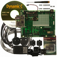
RCM3900 DEV KIT UNIVERSAL
Manufacturer
Rabbit Semiconductor
Series
RabbitCore 3900r
Type
MPU Moduler
Datasheet
1.20-101-1196.pdf
(168 pages)
Specifications of 101-1226
Contents
RabbitCore Module, Dev. Board, AC Adapter, Cable and Dynamic C® CD-Rom
For Use With/related Products
RCM3900
Lead Free Status / RoHS Status
Lead free / RoHS Compliant
Other names
316-1137


The Prototyping Board comes with the basic components necessary to demonstrate the
operation of the RCM3900. Four user LEDs (DS3–DS6) are connected to alternate I/O
bus pins PA0–PA3 pins of the RCM3900 module via U8, and may be driven as output
indicators when controlled by PE7 and PG5 as shown in the sample applications. Two
switches (S2 and S3) are connected to PG0 and PG1 to demonstrate the interface to the
Rabbit 3000 microprocessor. Reset switch S1 is the hardware reset for the RCM3900.
The Prototyping Board provides the user with RCM3900 connection points brought out con-
veniently to labeled points at J8 and J9 on the Prototyping Board. Although locations J8 and
J9 are unstuffed, 2 × 17 headers are included in the bag of parts.
RS-232 and RS-485 signals are available on screw-terminal header J14, quadrature
decoder inputs are available on screw-terminal header J5, and digital inputs are available
on screw-terminal header J6. A 1 × 5 header strip from the bag of parts may be installed at
J12 for four sinking digital outputs. The clocked Serial Port B signals from the RCM3900
are used for the microSD™ Card, and cannot be accessed via header J13 on the Prototyp-
ing Board.
If you don’t plan to use the LCD/keypad module, additional signals may be brought out on 1 × 5
and 1 × 8 headers from the bag of parts that you install at J15 and J16. If you don’t plan to
use the stepper-motor control option, additional CMOS outputs are available via a 1 × 8
header that you install at J10.
There is a through-hole prototyping space available on the Prototyping Board. The holes in
the prototyping area are spaced at 0.1" (2.5 mm). +3.3 V, +5 V, and GND traces run along
one edges of the prototyping area. Small to medium circuits can be prototyped using point-
to-point wiring with 20 to 30 AWG wire between the prototyping area, the +3.3 V, +5 V, and
GND traces, and the surrounding area where surface-mount components may be installed.
Small holes are provided around the surface-mounted components that may be installed
around the prototyping area.
B.4.1 Adding Other Components
There are two sets of pads for 6-pin, 16-pin, and 28-pin devices that can be used for sur-
face-mount prototyping devices. There are also pads that can be used for SMT resistors
and capacitors in an 0805 SMT package. Each component has every one of its pin pads
connected to a hole in which a 30 AWG wire can be soldered (standard wire wrap wire can
be soldered in for point-to-point wiring on the Prototyping Board). Because the traces are
very thin, carefully determine which set of holes is connected to which surface-mount pad.
RabbitCore RCM3900 User’s Manual
93
Related parts for 101-1226
Image
Part Number
Description
Manufacturer
Datasheet
Request
R

Part Number:
Description:
COMPUTER SNGLBD BL2120 FRCTNLOCK
Manufacturer:
Rabbit Semiconductor
Datasheet:

Part Number:
Description:
KIT APPLCTN RABBITCORE RCM4010
Manufacturer:
Rabbit Semiconductor
Datasheet:

Part Number:
Description:
KIT MESH NETWORK ADD-ON RCM4510W
Manufacturer:
Rabbit Semiconductor
Datasheet:

Part Number:
Description:
KIT DEV FOR BL2500 COYOTE
Manufacturer:
Rabbit Semiconductor
Datasheet:

Part Number:
Description:
KIT APPLICATION SIMPLE SENSOR
Manufacturer:
Rabbit Semiconductor
Datasheet:

Part Number:
Description:
KIT DEV RABBITCORE RCM3750
Manufacturer:
Rabbit Semiconductor
Datasheet:

Part Number:
Description:
KIT DEV RABBIT 2000 INT'L
Manufacturer:
Rabbit Semiconductor
Datasheet:
Part Number:
Description:
KIT DEV RABBIT RCM2000 INT'L
Manufacturer:
Rabbit Semiconductor
Datasheet:

Part Number:
Description:
KIT DEVELOPMENT RCM3700 INT'L
Manufacturer:
Rabbit Semiconductor
Datasheet:
Part Number:
Description:
MODULE RABBITCORE RCM3720
Manufacturer:
Rabbit Semiconductor
Datasheet:
Part Number:
Description:
MODULE RABBITCORE RCM3220
Manufacturer:
Rabbit Semiconductor
Datasheet:
Part Number:
Description:
MODULE RABBITCORE RCM3210
Manufacturer:
Rabbit Semiconductor
Datasheet:
Part Number:
Description:
COMPUTER SGL-BOARD OP6600 W/SRAM
Manufacturer:
Rabbit Semiconductor
Datasheet:
Part Number:
Description:
COMPUTER SGL-BD BL2000 SRAM/FLSH
Manufacturer:
Rabbit Semiconductor