DK-DEV-2AGX125N Altera, DK-DEV-2AGX125N Datasheet - Page 83
DK-DEV-2AGX125N
Manufacturer Part Number
DK-DEV-2AGX125N
Description
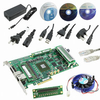
KIT DEV ARRIA II GX FPGA 2AGX125
Manufacturer
Altera
Series
Arria II GXr
Type
FPGAr
Datasheets
1.EP2AGX45CU17C6N.pdf
(96 pages)
2.DK-DEV-2AGX125N.pdf
(48 pages)
3.DK-DEV-2AGX125N.pdf
(64 pages)
Specifications of DK-DEV-2AGX125N
Contents
Board, Cables, CD, DVD, Power Supply
Silicon Manufacturer
Altera
Core Architecture
FPGA
Core Sub-architecture
Arria
Silicon Core Number
EP2
Silicon Family Name
Arria II GX
Rohs Compliant
Yes
For Use With/related Products
EP2AGX125EF35
Lead Free Status / RoHS Status
Lead free / RoHS Compliant
Other names
544-2600
Available stocks
Company
Part Number
Manufacturer
Quantity
Price
Company:

Part Number:
DK-DEV-2AGX125N
Manufacturer:
Altera
Quantity:
135


Chapter 1: Device Datasheet for Arria II Devices
Switching Characteristics
Table 1–61. Memory Output Clock Jitter Specification for Arria II GX Devices
Table 1–62. Memory Output Clock Jitter Specification for Arria II GZ Devices
December 2010 Altera Corporation
Duty cycle jitter
Notes to
(1) The memory output clock jitter measurements are for 200 consecutive clock cycles, as specified in the JEDEC DDR2/DDR3 SDRAM standard.
(2) The clock jitter specification applies to memory output clock pins generated using DDIO circuits clocked by a PLL output routed on a global
(3) The memory output clock jitter stated in
Clock period jitter
Cycle-to-cycle period jitter
Duty cycle jitter
Clock period jitter
Cycle-to-cycle period jitter
Duty cycle jitter
Notes to
(1) The memory output clock jitter measurements are for 200 consecutive clock cycles, as specified in the JEDEC DDR2/DDR3 SDRAM standard.
(2) The clock jitter specification applies to memory output clock pins generated using differential signal-splitter and DDIO circuits clocked by a
(3) The memory output clock jitter stated in
clock network.
PLL output routed on a regional or global clock network as specified. Altera recommends using regional clock networks whenever possible.
Parameter
Table
Table
Parameter
1–61:
1–62:
Table 1–62
Duty Cycle Distortion (DCD) Specifications
Table 1–63
Table 1–63. Duty Cycle Distortion on I/O Pins for Arria II GX Devices
Output Duty Cycle
Note to
(1) The DCD specification applies to clock outputs from the PLL, global clock tree, IOE driving dedicated, and general
Network
Global
Clock
purpose I/O pins.
Table
Regional
Regional
Regional
Symbol
Network
Global
Global
Global
Clock
lists the memory output clock jitter specifications for Arria II GZ devices.
lists the worst-case DCD specifications for Arria II GX devices.
1–63:
Table 1–61
Table 1–62
Symbol
t
JIT(duty)
is applicable when an input jitter of 30 ps is applied.
is applicable when an input jitter of 30 ps is applied.
Symbol
t
t
t
t
t
t
JIT(duty)
JIT(duty)
JIT(per)
JIT(per)
JIT(cc)
JIT(cc)
Min
45
-100
Min
C4
–4
Max
55
Max
100
-82.5
-82.5
-110
-165
Min
-55
-90
Arria II Device Handbook Volume 3: Device Datasheet and Addendum
Min
45
–3
I3, C5, I5
-125
Min
82.5
82.5
Max
110
165
55
90
Max
(Note
(Note
55
–5
1), (2),
Max
1), (2),
125
Min
45
-82.5
-82.5
-110
-165
Min
-55
-90
C6
(Note 1)
(3)
(3)
-125
Min
Max
(Part 2 of 2)
55
–4
–6
82.5
82.5
Max
110
165
55
90
Max
125
Unit
%
Unit
Unit
ps
ps
ps
ps
ps
ps
ps
1–75
Related parts for DK-DEV-2AGX125N
Image
Part Number
Description
Manufacturer
Datasheet
Request
R

Part Number:
Description:
KIT DEV CYCLONE III LS EP3CLS200
Manufacturer:
Altera
Datasheet:

Part Number:
Description:
KIT DEV STRATIX IV FPGA 4SE530
Manufacturer:
Altera
Datasheet:

Part Number:
Description:
KIT DEV FPGA 2AGX260 W/6.375G TX
Manufacturer:
Altera
Datasheet:

Part Number:
Description:
KIT DEV MAX V 5M570Z
Manufacturer:
Altera
Datasheet:

Part Number:
Description:
KIT DEV STRATIX V FPGA 5SGXEA7
Manufacturer:
Altera
Datasheet:

Part Number:
Description:
KIT DEVELOPMENT STRATIX III
Manufacturer:
Altera
Datasheet:

Part Number:
Description:
KIT DEVELOPMENT STRATIX IV
Manufacturer:
Altera
Datasheet:

Part Number:
Description:
KIT DEV ARRIA GX 1AGX60N
Manufacturer:
Altera
Datasheet:
Part Number:
Description:
KIT STARTER CYCLONE IV GX
Manufacturer:
Altera
Datasheet:
Part Number:
Description:
KIT DEVELOPMENT STRATIX IV
Manufacturer:
Altera
Datasheet:

Part Number:
Description:
CPLD, EP610 Family, ECMOS Process, 300 Gates, 16 Macro Cells, 16 Reg., 16 User I/Os, 5V Supply, 35 Speed Grade, 24DIP
Manufacturer:
Altera Corporation
Datasheet:
Part Number:
Description:
CPLD, EP610 Family, ECMOS Process, 300 Gates, 16 Macro Cells, 16 Reg., 16 User I/Os, 5V Supply, 15 Speed Grade, 24DIP
Manufacturer:
Altera Corporation
Datasheet: